D flip-flop - latch or delay element, Electrical Engineering

Assignment Help:

Q. D flip-flop - latch or delay element?

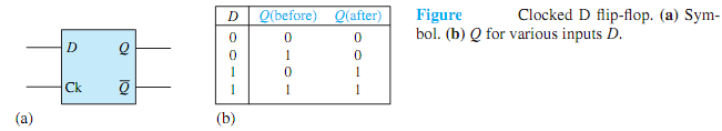
The symbol for the clocked D flip-flop is shown in Figure (a), in which the two output terminals Q and ¯ Q behave just as in the SRFF, and the input terminals are D and Ck (clock). The term clocked flip-flop indicates that this device cannot change its state (i.e., Q cannot change) unless a specific change instruction is given through the clock (Ck) input. The value of Q after the change instruction is equal to the value of D at the time the change instruction is received. The value of Q before the change instruction does not matter. Figure 6.1.20(b) illustrates the values taken by Q after the change instruction for various inputs D and prior values of Q. While there are several variations of the device, in the rising-edge triggered flip-flop a change instruction is effected whenever the Ck input makes a change from 0 to 1. Note that only a positive-going transition of Ck is a change instruction, and a constant Ck input is not a change instruction.

Note that flip-flops have propagation delay, whichmeans that there is a small delay (about 20 ns) between the change instruction and the time Q actually changes. The value of D that matters is its value when the change instruction is received, not its value at the later time when Q changes.

55_D flip-flop - latch or delay element.png

A convenient means of describing the series of transitions that occur as the signals set to the flip-flop input change is the timing diagram. A timing diagram depicts inputs and outputs (as a function of time) of the flip-flop (or any other logic device) showing the transitions that occur over time. The timing diagram thus provides a convenient visual representation of the evolution of the state of the flip-flop. However, the transitions can also be represented in tabular form.

Like logic blocks, flip-flops appear almost exclusively in IC form, and are more likely to be found in LSI and VLSI form. A very important application is in computer memories, in which a typical 256k RAM (random access memory) consists of about 256,000 flip-flops in a single IC.


Related Discussions:- D flip-flop - latch or delay element

Determine rc and resistance, Q. A silicon npn BJT is biased by the method s...

Q. A silicon npn BJT is biased by the method shown in Figure, with R E = 240 , R 2 = 3000 , and V CC = 24 V. The operating point corresponds to V BEQ = 0.8V, I BQ = 110 µA,

Successive approximation adc, Successive approximation ADC One method ...

Successive approximation ADC One method of addressing digital ramp ADC's shortcomings is so-called successive approximation ADC. Only change in this design is a very special c

Latch - introductio to microprocessors , Latch A 8 bit  latch comprise...

Latch A 8 bit  latch comprises of transparent latch D flip  flop. It is commonly  used  to interface output  device with  microprocessor. A typical example of such 8 bit  latc

Variation of energy bands with alloy composition, Variation of Energy Bands...

Variation of Energy Bands with Alloy Composition The  band  structures  of  III-V  ternary  and  quaternary  compounds  modifies  as  their composition is varied. There

Sign flag - sub subtract instruction , Sign flag Since D 7  bit in ...

Sign flag Since D 7  bit in the  results is 0sign flag is reset. This also  shown that the results is positive.

Phenomenon - fet operation, Phenomenon - Fet operation: For either imp...

Phenomenon - Fet operation: For either improvement- or depletion-mode devices, at drain-to-source voltages very much less than gate-to-source voltages, changing the gate volta

Working principle of an electronic voltmeter, Q.   Explain the working prin...

Q.   Explain the working principle of an electronic voltmeter. Sol. Electronic voltmeter Basic Voltmeter: The addition of a series resistor, or multiplier, converts the

Compute the induced emf, Compute the induced emf: If a coil of 150 tur...

Compute the induced emf: If a coil of 150 turns is linked with a flux of 0.01 wb while carrying a current of 10 Amp, compute the inductance of coil. Now, if current is reverse

Construct a suitable piecewise linear equivalent circuit, Problem: The ...

Problem: The current voltage characteristic [ ID versus VD] of a semiconductor diode for VD > 0 [forward bias] is given in Figure Under reverse bias conditions [VD Fi

Explain instruction sets of 8085, Explain instruction sets of 8085. a) ...

Explain instruction sets of 8085. a)  Data transfer group - MOV, MVI, LXI. b)  Arithmetic group - ADD, SUB, INR. c)  Branch group - JMP, JNZ, CALL. d)  Logical group -

Write Your Message!

Captcha
Free Assignment Quote

Assured A++ Grade

Get guaranteed satisfaction & time on delivery in every assignment order you paid with us! We ensure premium quality solution document along with free turntin report!

All rights reserved! Copyrights ©2019-2020 ExpertsMind IT Educational Pvt Ltd