Basic characteristics and operation of mosfet, Electrical Engineering

Assignment Help:

Q. Basic Characteristics and Operation of MOSFET ?

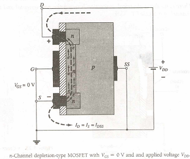
In Figure the gate-to-source voltage is set to zero volts by the direct connection from one terminal to the other, and a voltage V DS is applied across the drain-to-source terminals. The result is an attraction for the positive potential at the drain by the free electrons of the n- channel and a current similar to that established through the channel of the JFET. In fact, the resulting current with VDS = 0 V continues to be labeled IDss, as shown in Figure.

166_Basic Characteristics and Operation.png

In Figure, VDS has been set at a negative voltage such as -1 V. The negative potential at the gate will tend to pressure electrons toward the p-type substrate (like charges repel) and attract holes from the p-type substrate (opposite charges attract) as shown in Figure.

Depending on the magnitude of the negative bias established by VDS, a level of recombination between electrons and holes will occur that will reduce the number of free electrons in the n-channel available for conduction. The more negative the bias, the higher the rate of recombination. The resulting level of drain current is therefore reduced with increasing negative bias for VDS as shown in Figure for VDS = -1V,-2V, and so on, to the pinch-off level of - 6 V. The resulting levels of drain current mid the plotting of the transfer curve proceeds exactly as described for the JFET.

For positive values of V GS' the positive gate will draw additional electrons (free carriers) from the p-type substrate due to the reverse leakage current and establish new carriers through the collisions resulting between accelerating particles. As the gate-to-source voltage continues to increase in the positive direction, the drain current will increase at a rapid rate for the reasons listed above. The  vertical spacing between the V GS = 0 V and V GS = + 1 V curves of Fig is a clear the application of a voltage V GS = + 4 V would result in a drain current of 22.2 mA, which could possibly exceed the maximum rating (current or power) for the device. As revealed above, the application of a positive gate-to-source voltage has "enhanced" the level of free carriers in the channel compared to that encountered with V GS = 0 V.


Related Discussions:- Basic characteristics and operation of mosfet

Multiprogramming - single processor one users many program, Multiprogramm...

Multiprogramming - Single Processor one Users  Many  Programs When single  processor is  used to execute more than  one independent program simultaneously the technique  is ca

Encoder - introduction to microprocessors , Encoder The encoder is a...

Encoder The encoder is a logic  circuit  which  provides  the binary code is  output  for each input each input signal. In  other words  we can  say that it performs  just  op

Ic packaging, which type of ic package is more advantageous,suitable and ve...

which type of ic package is more advantageous,suitable and versatile

Find the line current and voltage across the load, Q. (a) A balanced wye-co...

Q. (a) A balanced wye-connected load with per-phase impedance of 20 + j10 is connected to a balanced 415-V, three-phase supply through three conductors, each of which has a series

Singles phase half wave controlled rectifier with rl load, Singles Phase ...

Singles Phase  Half wave Controlled Rectifier  with RL Load When gate pulses are applied to the thyristor  at output voltage  v0 follows the input voltage  v s ( = V m sin ) s

Briefly discuss about cascaded amplifier, Q. Briefly discuss about ‘Cascade...

Q. Briefly discuss about ‘Cascaded Amplifier' using a diagram? Amplifiers are cascaded when the output of the first is the input to the second. The combined gain is whe

Derating factor, Conductors with a temperature rating of 75 degrees C are r...

Conductors with a temperature rating of 75 degrees C are run in an area with an ambient temperature of 55 degrees C. What would be the de-rating factor that should be applied?

LED, what ternary alloy, composition and binary substrate can be used for ...

what ternary alloy, composition and binary substrate can be used for an LED at 1.55 µm optical fiber windo

Write Your Message!

Captcha
Free Assignment Quote

Assured A++ Grade

Get guaranteed satisfaction & time on delivery in every assignment order you paid with us! We ensure premium quality solution document along with free turntin report!

All rights reserved! Copyrights ©2019-2020 ExpertsMind IT Educational Pvt Ltd