Amplifiers with feedback, Electrical Engineering

Assignment Help:

Q. Amplifiers with Feedback?

Almost all practical amplifier circuits include some form of negative feedback. The advantages gained with feedback may include the following:

• Less sensitivity to transistor parameter variations.

• Improved linearity of the output signal by reducing the effect of nonlinear distortion.

• Better low- and high-frequency response.

• Reduction of input or output loading effects.

The gain is willingly sacrificed in exchange for the benefits of negative feedback. Compensating networks are often employed to ensure stability.Avoltage amplifierwith negative feedback is shown by the generalized block diagram in Figure. The negative feedback creates a self - correcting amplification system that compensates for the shortcomings of the amplifying unit.

The gain with feedback can be seen to be

512_Amplifiers with Feedback.png


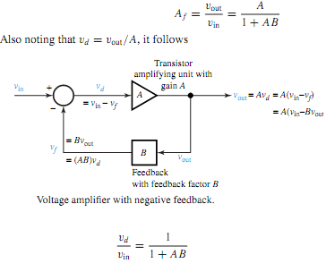
The product AB is known as the loop gain because vf = B(Avd ) = (AB)vd . In order to obtain negative feedback, the loop gain must be positive. With AB > 0 in Equation it follows that |Af | < |A|. Thus, a negative feedback amplifier has always less gain than the amplifying unit itself. With AB >> 1, Af remains essentially constant, thereby reducing the effect of transistor parameter variations in the amplifying unit. If the feedback unit has |B| < 1, one can still obtain useful amplification since |Af | = 1/|B| > 1.

These are also known as RC amplifiers since their circuits need only resistors and capacitors. There are of course other transistor amplifiers that do not have the small-signal limitation and are also not limited to the use of resistors and capacitors in their circuits. For larger input signals the linear dependence of the current on the signal level may not be maintained.


Related Discussions:- Amplifiers with feedback

Theoretical circuit, Theoretical Circuit The theoretical circuit is ava...

Theoretical Circuit The theoretical circuit is available in form 1.Passive materials with mediocre dimension is used by the manufacturer. In order to make a theoretical circuit

Binary multiplication, Q. What do you mean by Binary Multiplication? Th...

Q. What do you mean by Binary Multiplication? The Rules of Binary Multiplication 0 x 0 = 0 0 x 1 = 0 1 x 0 = 0 1 x 1 = 1 , and no carry or borrow

Effect of temperature on resistivity of conducting materials, Explain the e...

Explain the effect of temperature on the resistivity of conducting materials. The resistance of most metals rises with rise of temperature whereas that of semiconductors and el

Explain time multiplexed space switching, Explain time multiplexed space sw...

Explain time multiplexed space switching? With a neat diagram illustrate its operation. Ans: Time division switches where an outlet or an inlet corresponded to a single s

Abcd propagation , ABCD propagation of an optical ray through a system can...

ABCD propagation of an optical ray through a system can be explained by a simple 2_2 matrix. In ray optics, the characteristic of a system is given by the corresponding ray matrix

Determine the voltages, Question: a) For the circuit shown in figure ...

Question: a) For the circuit shown in figure (i) Determine the voltages across R1 and R2 and (ii) Determine the current which flows across R1 and R2. Both D1 and D2 a

Calculate the current flowing through the inductor, The circuit is altered ...

The circuit is altered by replacing the capacitor, C1 with an inductor of 150mH and left with the switch in position (a) for a long time. At time t=0, the switch is moved from posi

Equivalent resistor reductions for the circuit, Q. Determine the voltages V...

Q. Determine the voltages V x using voltage division and equivalent resistor reductions for the circuits shown in Figure.

Voltage tripler and quadrupler, Voltage Tripler and Quadrupler: Voltag...

Voltage Tripler and Quadrupler: Voltage Tripler an extension of the half wave voltage across each diode is 2Vm as it is for the filter capacitor circuit. It should be obvious

Design of matching networks for amplifiers, Design a low noise amplifier us...

Design a low noise amplifier using an Infineon RF transistor BFP640. The amplifier is to be used to amplify the L2 GPS signal and so the centre frequency is 1227MHz and bandwidth 4

Write Your Message!

Captcha
Free Assignment Quote

Assured A++ Grade

Get guaranteed satisfaction & time on delivery in every assignment order you paid with us! We ensure premium quality solution document along with free turntin report!

All rights reserved! Copyrights ©2019-2020 ExpertsMind IT Educational Pvt Ltd