Address phase timing - computer architecture, Computer Engineering

Assignment Help:

Address phase timing:

On the rising edge of clock 0, the initiator notes IRDY # and FRAME# both high, and GNT# low, so it drives the command, address and asserts FRAME# in time for the rising edge of c lock 1. Targets latch the address and start decoding it. They can respond having DEVSEL# in time for clock 2 (fast DEVSEL), 3 (medium) or 4 (slow). Subtractive decode devices, by seeing no other response by clock 4, may respond on clock5. If the master does not observe a response by clock 5, it will dismiss the transaction and remove FRAME# on clock 6.


2223_Address phase timing.png

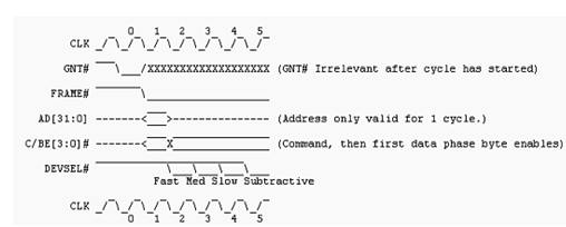
TRDY# and STOP# are deserted (high) during the address phase. The initiator can assert IRDY# as soon as it is prepared to transfer data, which could theoretically beat the time clock 2.

Arbitration:

Any particular device on a PCI bus that is capable of acting as a bus master can initiate a transaction having any other device. To ensure that only 1 transaction is initiated at a time, each master have to wait first for a bus grant signal, GNT#, from an arbiter located on the motherboard. Each device has a distant request line REQ# that requests the bus, but the arbiter may "park" the bus grant signal at any device if there are no present requests. The arbiter can remove GNT# at any particular time. A device which loses GNT# may complete its existing transaction, but may not begin one (by asserting FRAME#) unless it observes GNT# asserted the cycle before it start.

The arbiter can also provide GNT# at any particular time, by including during another master's transaction. At the time of transaction, either FRAME# or IRDY# or both are asserted; when both are deserted, the bus is id le. A device can initiate a transaction at any time that GNT# is asserted and the bus is idle.


Related Discussions:- Address phase timing - computer architecture

How to convert binary to octal and hexadecimal, Q. How to convert Binary to...

Q. How to convert Binary to Octal and Hexadecimal? Rules for these conversions are simple. For converting binary to octal binary number is splitted in groups of three, that are

Explain what logic gets synthesized , What logic gets synthesized when I us...

What logic gets synthesized when I use an integer instead of a reg variable as a storage element? Is use of integer recommended? An  integer  can  take  place  of  a  reg  as

Micooperation, please suggest me ,how to write microopertions,and study for...

please suggest me ,how to write microopertions,and study for computer architecture

Economic argument for good design, One way of demonstrating the importance ...

One way of demonstrating the importance of good ID is by showing tangible benefits that can be talked about in cash terms. Within a business, good ID can lead to benefits such as h

Define the concept of typing of object oriented analysis, Define the concep...

Define the concept of Typing of object oriented analysis Typing enforces object class such that objects of different classes cannot be interchanged.  Or we can say that, class

What is system conception, What is system conception? It deals with gen...

What is system conception? It deals with genesis of an application and formulating tentative needs. The purpose of the system conception is to defer details and understand what

Events by which we can program "help texts", What are the events by which w...

What are the events by which we can program "help texts" and display "possible value lists"? -PROCESS ON HELP-REQUEST (POH). -PROCESS ON VALUE-REQUEST (POV).

Explain about flip-flops, Explain about Flip-Flops  Flip-Flops are also...

Explain about Flip-Flops  Flip-Flops are also called bistable multivibrator.  A flip-flop is capable of storing 1 bit of binary data.  It has two stable states- 'one' and 'zero

Illustrate cache dram, Q. Illustrate Cache DRAM? Cache DRAM (CDRAM) wh...

Q. Illustrate Cache DRAM? Cache DRAM (CDRAM) which is developed by Mitsubishi integrates a tiny SRAM cache (16Kb) on a generic DRAM chip. SRAM on the CDRAM can be used in two

Design odd-even transposition algorithm, Q. Design Odd-Even Transposition A...

Q. Design Odd-Even Transposition Algorithm? Algorithm: Odd-Even Transposition for I=1 to N     {            If (I%2 != 0) //i.e. Odd phase            {

Write Your Message!

Captcha
Free Assignment Quote

Assured A++ Grade

Get guaranteed satisfaction & time on delivery in every assignment order you paid with us! We ensure premium quality solution document along with free turntin report!

All rights reserved! Copyrights ©2019-2020 ExpertsMind IT Educational Pvt Ltd