8255 programmable peripheral interface-microprocessor, Assembly Language

Assignment Help:

8255 Programmable Peripheral Interface

Intel's 8255 A programmable peripheral interface provides a nice instance of a parallel  interface. As shown the interface have a control register and 3 separately addressable ports, denoted from A, B, and C. Whether or not an 8255A is being accessed is determined by the signal on the CS pin and the direction of the access is according to the WR and RD signals. Which of the 4 registers is being addressed is determined by the signals applied to the pins A0 and A1. So, the lowest port address assigned to an 8255 A might be divisible by 4. A review of the 8255 A's addressing is:

A1        A0        RD       WR      CS        Transfer Description

0          0          0          1          0          Port A to data bus

0          1          0          1          0          Port B to data bus

1          0          0          1          0          Port C to data bus

0          0          1          0          0          Data bus to port A

0          1          1          0          0          Data bus to port B

1          0          1          0          0          Data bus to port C

1          1          1          0          0          Data bus to control register if D7= 1; if D7=0 input from the data bus is treated as a Set/Reset instruction

x          x          x          x          1          D7-D0 go to high-impedance state

1          1          0          1          0          Illegal combination

x          x          1          1          0          D7-D0 go to high-impedance state

Where 0 is low and 1 is high

Because the bits in port C are sometimes utilized as control bits, the 8255 A is designed so that they may be output to separately by using a Reset/set instruction. When the 8255 A receives a byte that is directed to its control register, it checked data bit 7.If this bit is one, the data are transferred to the control register, but if it is zero, the data retreated as a Reset/set instruction and is utilized to clear or set the port C it denoted by the instruction. Bits 3-1 gives the bit number of the bit to be changed and bit 0 denote whether it is to be cleared or set. The remaining bits are not useful.

535_8255.jpg

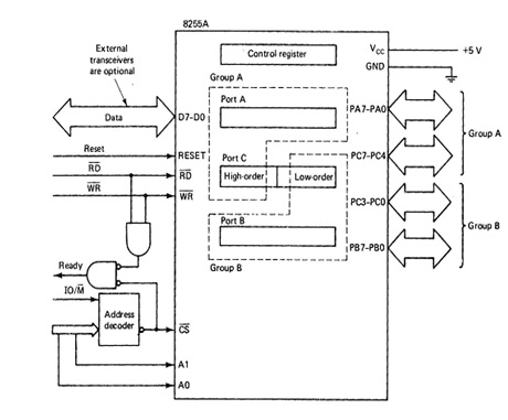
The bits in the 3 ports are attached to pins that can be linked to the I/O device. These bits are divided into groups A & B, with group A consisting of the bits in port A and the 4 MSBs of port C and group b consisting of port B and the 4 LSBs of port C. the use of each of the 2 groups is controlled by the mode connected with it. Group A is connected with 1 of 3 modes, mode zero, mode one, and mode two, and group B with 1 of 2 modes, mode 0 and mode 1.


Related Discussions:- 8255 programmable peripheral interface-microprocessor

Test-logical instruction-microprocessor, TEST : Logical Compare Instructio...

TEST : Logical Compare Instruction: The TEST instruction performs bit by bit logical AND operation on the 2 operands. Each bit of the result is then set to value I, if the equival

Opcode-microprocessor, Opcode : The opcode generally appear in the firs...

Opcode : The opcode generally appear in the first byte.but in a few instructions, a register objective is in the first byte and few other instructions may have their 3-bits of

2 homework assignements, I have two homework assignments due in 10 hours fo...

I have two homework assignments due in 10 hours for the x86 processor assembly language

The pin diagram of 8088-microprocessor, Pin diagram of 8088 : The pin ...

Pin diagram of 8088 : The pin diagram of 8088 is shown in given figure. Most of the 8088 pins and their functions are exactly similar to the corresponding pins of 8086.  Hence

Develop a schematic circuit diagram of system, Develop a suitable schematic...

Develop a suitable schematic circuit diagram of your system showing the interface between the PIC16F84 and the existing mains light & switch, including 5V derivation from the 240V

Assembly help, use">http://www.raritanval.edu/uploadedFiles/faculty/cs/full...

use">http://www.raritanval.edu/uploadedFiles/faculty/cs/full-time/Brower/CISY256/2013Spring/CISY256%20Assembly%20Project.pdf use microsoft visual 2010 and http://www.asmirvine.c

.., Sum of series of 10 numbers and store result in memory location total

Sum of series of 10 numbers and store result in memory location total

Display control-microprocessor, Display control 8279  provides  a  16  ...

Display control 8279  provides  a  16  byte  display  memory  and  refresh  logic.  Every address in the display memory corresponds to a display unit with address zero represen

Segment registers-microprocessor, Segment Registers The 8086 addresses ...

Segment Registers The 8086 addresses a segmented memory unlike 8085. The complete 1 megabyte memory, which 8086 is capable to address is divided into 16 logical segments.Thusea

Plus and underline , What is the hex for + and - under with a sum involved

What is the hex for + and - under with a sum involved

Write Your Message!

Captcha
Free Assignment Quote

Assured A++ Grade

Get guaranteed satisfaction & time on delivery in every assignment order you paid with us! We ensure premium quality solution document along with free turntin report!

All rights reserved! Copyrights ©2019-2020 ExpertsMind IT Educational Pvt Ltd