8254 Programmable Timer
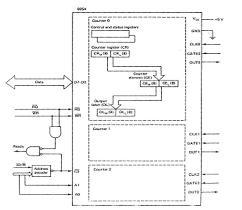
A diagram of Intel's 8254 interval event/timer counter is given in Figure. The 8254 consists of 3 identical counting circuits, per of which has GATE and CLK inputs and an OUT output. Each may be viewed as containing a status and control Register pair, a Counter Register (CR) for receiving the initial count, a Counter Element (CCE) which performs the counting but it is not directly accessible from the processor, and from an Output Latch (OL) for latching the contents of the CE so that they may be read. The CE, CR, and OL are treated as pairs of 8-bit registers. (Physically, the registers are not accurately as depicted, but to the programmer the figure is conceptually accurate.)
The registers might be accessed according to the table given below:
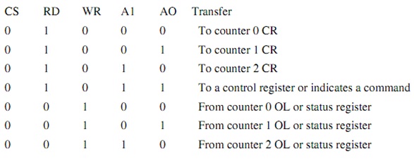
Where zero means low and one means high. All combinations result in the data pins being put into their high-impedance state. When A1 = 1 and A0=1, whether a control register is being written into or a command is depends on the MSBs of the byte being output. For the last 3 combinations, whether an OL or status register is read is determined by a previous command.
There are 2 types of commands, the counter latch command, which causes the CE in the counter indicated by the 2 MSBs of the command to be latched into the corresponding OL, and the read back command, which might cause a combination of the CEs to be latched or "prepare" a combination of status registers to be read. For the purpose to prepare a status register means to cause it to be read the next time a read operation inputs from the counter. When the2 MSBs are 01, 00, or 10 a counter latch command is mention, but if they are 11 a read back is to be performed. In a latch command bits five and four might be zero and the remaining bits are unused. The read back command format is given below:
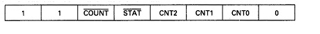
If the COUNT bit is zero, then the CEs for all of the counters whose CNT bits are one are latched. If CNTO= 1 &CNT2=1 but CNT1=0, then the CEs in counters zero and two are latched but the CE in counter one is not latched. likewise STAT=0 causes the counters' status registers to be prepared for input. CEs may be and status and latched registers may be prepared in the similar command.
The formats of the status and command registers are given in Figure. If the 2 MSBs of an output are both one, they denoted that the output is to be a read back command; or else they indicate a counter. If they indicate a counter and bits four and five are both zero, then a latch command is denoted and it is directed to the control register of the counter indicated by the top two bits, but if they are not both zero, then they denote the type of the input from OL or output to CR. The combination 01 denoted that the Read/Write operations are from/to the OLL/CRL, 10 denoted that they are to/from the OLM/CRM, and 11 denoted that these operations are to occur in pairs, having the first byte coming from/going to OLL/CRL and the second from/to OLM/CRM. A 1-byte write to CR will cause the other byte to be 0. Bits 1, 2, and 3 determine the mode and bit 0 indicate the format of the count.