8088 timing system diagram-Microprocessor, Assembly Language

Assignment Help:

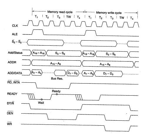
8088  Timing System Diagram

The 8088 address/data  bus is divided  in 3 parts (a) the lower 8 address/data  bits, (b) the middle 8 address bits, and (c) the upper 4 status/address bits. The lower 8 lines are time multiplexed for data bus and address bus. The upper 4 lines are time multiplexed for address bus and status bus. Each of the bus cycles has T1, T2, T3, T4 and Tw states. The ALE signal goes high for one clock cycle in T1. The trailing edge of ALE is used to latch the valid addresses available on the multiplexed lines. They remain valid above the bus for the next cycle (T2). The middle 8 address bits are always present on the bus throughout the bus cycle. The lower order address bus is tristated after T2 to change its direction for read data operation. The real data transfer takes place during T4 and T3. Hence the data lines are valid in T3 / T4. The multiplexed bus is tristated again to be ready for the next bus cycle. The status lines are valid for the multiplexed address/status bus for T2, T3 and T4 clock cycles.

In case of write cycle, the timing diagram is similar to the read cycle except for the validity of data. The data bits are available in the write cycle on the bus for T2, T3, T4, and Tw. At the end of 14, the bus is tristated. The other signals WR, RD, INTA, DT/R, READY and DEN are similar to the 8086 timing diagram. Figure shows the details of read and writes bus cycles of 8088.

2332_8088 timing system.jpg

With an 8-bit external data bus, the 8088 has been designed for internal  16-bit  processing  capability. Closely all the internal functions of 8088 are equal to 8086. The 8088 utilized the external bus in the similar way as 8086, but only 8 bits of external data are accessed at a time. While writing or fetching the 16-bit data, the job is performed in 2 consecutive bus cycles. As the software is concerned, the chips are equal except in case of timings. The 8088, thus might take more time for execution of a particular task as compared to 8086.


Related Discussions:- 8088 timing system diagram-Microprocessor

Operating System, Why is the capability to relocate processes desirable?

Why is the capability to relocate processes desirable?

General data registers-microprocessor, General Data Registers Given fig...

General Data Registers Given figure indicate the register organization of 8086. The registers DX, CX, BX and AX are the general purpose 16-bit registers. AX is behaved as 16-bi

Mouse, hey ,, I need to know how to let a symbol moves with mouse ??

hey ,, I need to know how to let a symbol moves with mouse ??

Addressing modes for sequential control-microprocessor, The addressing mode...

The addressing modes for the sequential control transfer instructions are described below:   1. Immediate: Immediate data is a part of instruction,in this type of addressin

Summation Program., Write a program to solve problem 9, Summation Program, ...

Write a program to solve problem 9, Summation Program, on page 179 of chapter 5 in the textbook (book:kip Irvine Assembly Language sixth edition)

Program for initialize two row lcd, init_lcd                        ;(this ...

init_lcd                        ;(this initialises a 2 row lcd)     bcf     TRISA,0             ;PORTA bit 0 as an output (lcd RS pin)     bcf     TRISA,1             ;PORTA bit 1

Physical memory mapped and port input output-microprocessor, Physical Memor...

Physical Memory Mapped I/O and Port I/O : CPU controlled I/O comes in 2 ways. Simply the difference is whether we utilize the normal memory addresses for I/O, this is mention

Cisc characteristics-microprocessor, CISC Characteristics : The design...

CISC Characteristics : The design of an instruction  set for a computer  might take into consideration  not only machine language constraints,  but  also  the  requirements  i

External hardware-interrupts-microprocessor, External Hardware-Interrupts ...

External Hardware-Interrupts External hardware-interrupts are generated by controllers of external devices or coprocessors and are connected to the processor pin for Non Mask a

Read architecture:look aside cache-microprocessor, Read Architecture : Look...

Read Architecture : Look Aside Cache In "look aside" cache architecture the main memory is located conflictingthe system interface. Both the cache main memory sees a bus cycle

Write Your Message!

Captcha
Free Assignment Quote

Assured A++ Grade

Get guaranteed satisfaction & time on delivery in every assignment order you paid with us! We ensure premium quality solution document along with free turntin report!

All rights reserved! Copyrights ©2019-2020 ExpertsMind IT Educational Pvt Ltd