Reference no: EM131085057
Microprocessors
Lab: Bread boarding Technique Review
"Without minute neatness of execution, the sublime cannot exist. Grandeur of ideas is founded on precision of ideas."
-- William Blake
Objectives:
To review breadboarding and unit-testing techniques, in order to prepare for the construction of the DrACo/Z80 computer.
WARNING! MAKE SURE ALL SOURCES ARE SET TO "+5V" OR "TTL." OTHERWISE, IT MIGHT LET ALL OF THE MAGIC BLUE SMOKE OUT!
Exercise 1. Load and Store
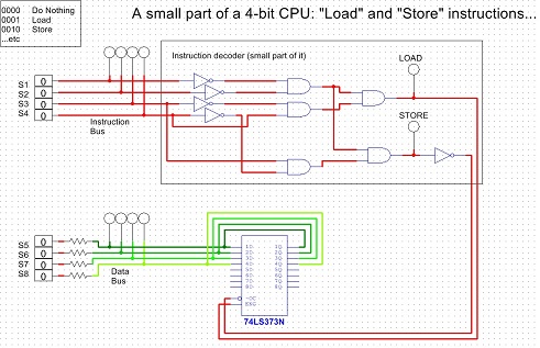
In this exercise, you will wire up a 74AHC373N chip as an eight-bit load/store register, according to the schematic in Figure 1, below.
NEATNESS COUNTS! After this lab, we will start building a Z80-based computer.
Neat, reliable wiring techniques and unit-testing are essential. If you build the whole computer without testing it, it almost certainly will not work, and will be a nightmare to troubleshoot and get working. Practice neatness and unit testing in this lab, and make a habit of them when you build the DrACo/Z80. It will make your life a lot easier!
BEFORE YOU BUILD ANYTHING, go through the schematic and plan which gates on which chips you will use for each logic gate shown. Look at the pinouts of your chips, and try to decide what will make the most sense. (For example, look at the two AND gates near the top right part of the LOAD circuit. One of these feeds the other, so it would make sense for those to be either gates A and B or gates C and D of a single chip. Since the output of gate A is right next to the input of gate B, you can use a single 0.1" connector to make the link. Nice, neat - and most importantly, easy to troubleshoot!
Similarly, try to locate chips near others that connect to them, group related bunches of wires together, etc.
First, create the Instruction Decoder logic. You will need a single 74LS04 inverter chip and two 74LS08 quad AND chips. The resistors shown in the schematic are all 1k.
Once you have the logic assembled, unit-test it. The "LOAD" light should go on for opcode 0001, and the "STORE" light should go on for opcode 0010. (You can use LEDs in series with 330-ohm resistors for this.)
Once your logic is tested and working (ask me or the TA if you're unsure), you can connect up the ‘373 chip. REMEMBER TO INCLUDE THE RESISTORS in line with logic switches S5 through S8, so as not to burn out the chip or Cadet trainer board!
Please ask me or your TA to check your circuit before you power it on.
Once your circuit is built and verified, try "loading" the chip using opcode 0001, and "storing" the output back onto the data bus, using opcode 0010. This should work like the example in lecture.
TIP: Take care not to bend the pins when inserting the chips. If the pins are splayed outward (they usually are when the chips are new), use a chip pin straightener tool to correct this. (If you have any questions, please ask.)
Remember to connect power and ground to all chips (not shown on the schematic.)

Figure 1. The schematic for a load/store setup using a ‘373 chip.
LAB WRITEUP:
You can write an informal report for this lab only. Just tell the story of what you did.
Please make sure you include somewhere in your report:
• A description of what you built;
• A photo of your completed circuit;
• A description of how it works;
• What unit testing techniques you used and why;
• What techniques you used to improve the layout;
• Your thoughts on what else could be done to make the layout neater.