Reference no: EM132916115
In this lab, the students will obtain experience with sequential logic design, and study digital design using the Xilinx design package for FPGAs. It is assumed that students are familiar with the operation of the Xilinx design package for Field Programmable Gate Arrays (FPGAs) through the Xilinix tutorial available in the class website.
1. This lab introduces unsigned binary division algorithms, including the restoring algorithm.
2. Given a dividend ‘a' and a divisor ‘b', the restoring division algorithm calculates the quotient ‘q' and the remainder ‘r' such that a = b x q + r and r < b, by subtracting b from the partial remainder (initially the MSB of a). If the result of the subtraction is not negative, we set the quotient bit to 1. Otherwise, b is added back to the result to restore the partial remainder. Then we shift the partial remainder with the remaining bits of ‘a' to the left by one bit for the calculation of the next quotient bit. This procedure is repeated until all the bits of ‘a' are shifted out.
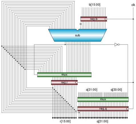
3. Figure 1 shows the schematic diagram of a restoring divider. There are three registers: reg_b, reg_r, and reg_q, for storing the divisor b, a remainder r, and quotient q respectively. Initially, reg_q stores the dividend a. A subtracter is used to subtract b from the partial remainder. The MSB of the output of the subtracter is used to determine whether the result of the subtraction is negative or not. The multiplexer over reg_q is used to load a initially and to shift the content of reg_q (a and q) to the left later. The multiplexer over reg_r implements the restoring. If the result of the subtraction is negative, the multiplexer selects the original partial remainder. Otherwise, it selects the result of the subtraction. At each iteration, one bit of q is obtained from the sign bit of the subtracter result and written to the LSB of the reg_q.
4. In Figure 2, start signal means the start of the division; busy indicates that the divider is busy (can't start a new division); ready indicates that the quotient and remainder are available; and count is the output of a counter that is used to control the iterations of the division.
5. Figure 2 shows part of the expected output of the simulation of 0x4c7f228a / 0x6a0e, q = 0xb8a6 and r = 0x4d76 are available when ready is 1 at 330 ns and then 0xffff00/4, q is 0x3fffc0, and r is 0

Figure 1 Schematic diagram of a restoring divider

Figure 2 Part of the expected output.
6. Write a behavioral Verilog code describing Figure 1. Compile and simulate your code to correctly do the division.
7. Write a report that contains the following:
a. Your Verilog design code. Use:
i. Device: XC7Z010- -1CLG400C or choose any other FPGA type. You can use Arria V if you are using Quartus II software.
b. Your Verilog Test Bench design code to do the following division shown in item 5 (0x4c7f228a / 0x6a0e). Add "`timescale 1ns/1ps" as the first line of your test bench file.
c. The waveforms resulting from the verification of your design with the simulation software, showing all the signals as shown in Figure 2. Show the signals till 680 ns.
d. The design schematics from the synthesis of your design. Do not use any area constraints.
e. Snapshot of the I/O Planning and
f. Snapshot of the floor planning