Reference no: EM132152790
Practical - Diodes and Amplifiers
Building and testing
Part - Half-wave rectifiers
In this section, you will be building and testing a diode circuit known as a half-wave rectifier. A rectifier is an electrical device that converts an alternating current (AC) signal, which periodically reverses direction, to a direct current (DC) signal, which only flows in one direction. This process is known as rectification, and as the name suggests, a half-wave rectifier only rectifies half of the AC wave. Figure 2.1 shows the circuit diagram for this section.
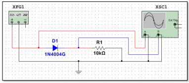
Figure 2.1 - Example of a half-wave rectifier circuit
1. Start with a clean, empty breadboard.
2. In this circuit, you will need:
• 1 x 1N4004 diode
• 1 x 10 k? resistor
• 1 x Function generator
• 1 x Oscilloscope (2 channels)
3. Change the parameters on the function generator so that it is outputting a Sine wave with frequency of 50 Hz, amplitude of 5 VPP, offset of 0 VPP, Make sure that the OUTPUT is turned off.
4. As you would have learnt in the previous practical, diodes are polarised components. Figure 2.2 is a refresher for how the physical component relates to the circuit diagram.
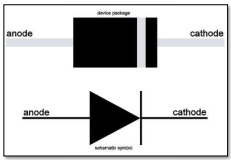
Figure 2.2 - Diode polarisation
5. Wire up the circuit so that the function generator is outputting a waveform through the diode in forward bias, through a 10 k? resistor in series, and finally to GROUND.
6. Connect channel 1 of the oscilloscope so that it is measuring the output of the function generator. Connect channel 2 so that it is measuring the voltage across the resistor.
7. In your previous practical, you used the AUTO function on the oscilloscope to scale the waveforms to the screen. In this practical, you will instead be using the manual scaling controls of the oscilloscope.
8. Turn the OUTPUT of the function generator on, press AUTO on the oscilloscope, and observe the waveforms. It is much easier to compare these waveforms if they are displayed in the same position vertically. Figure 2.3 shows the controls on the oscilloscope relating to the vertical display. The smaller dial on the top adjusts the position of the waveform, and the larger dial on the bottom adjusts the scale.
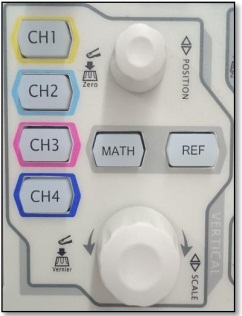
Figure 2.3 - Oscilloscope vertical display controls
9. To set the vertical position quickly, first press the channel button to select that channel, and then press the smaller dial to zero the position.
10. Next, adjust the scale so that the waveform takes up as much of the screen as possible while still remaining on the screen entirely. For the parameters of this section, 1.00 V (display on the bottom left of the screen) scales the waveform quite nicely.
11. Repeat these steps for the other channel, making sure that the scale is identical.
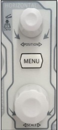
Figure 2.4 - Oscilloscope horizontal display controls
12. With the vertical axes set, you now need to adjust the horizontal axes. On this oscilloscope, the horizontal axis is identical for all waveforms. Figure 2.4 shows the controls that relate to the horizontal axis settings, where the dials perform the same actions as the vertical controls.
13. Adjust the scale of the horizontal axis to 10.0 ms (shown along the top left of the oscilloscope display) and confirm that the waveform is repetitive. Now, adjust the scale to 2.00 ms, which shows the maximum amount of detail for both waveforms, while ensuring that they have at least one full period shown.
14. The last control that you need to know about is the trigger control, which sets the point at which the oscilloscope will update the display constantly.

Figure 2.5 - Oscilloscope trigger controls
15. The oscilloscope should default to the ‘Auto' setting, as seen in Figure 2.5. If this is not correct, press the MODE button until it is.
16. Depending on the circuit, you may need to set the trigger to a specific channel. In this practical, you need to set the trigger to channel 1. To do this, press the MENU button on the trigger controls, and ensure that the ‘Source' option on the screen is set to CH1. If it isn't, change it now.
17. As you adjust the trigger dial, you should notice that the waveform moves. The trigger is relatively to the centre of the screen. If you press the trigger dial down, it will zero the trigger level. The waveform of channel 1 should now be crossing the intersection of both axes in the middle of the screen.
18. To show what happens when you have the trigger set incorrectly, change the trigger Source to CH2.
19. Set the trigger Source back to CH1.
20. Move the cursor on the oscilloscope so that you are measuring the peak voltages of both channels. Save this waveform, put it in your report, and report the peak voltage of both channels
21. Why is there a difference between the amplitudes?
22. What is the frequency of the output wave?
23. Is there a phase difference between the input and output signals? Why?
Part 2b Full-wave rectifiers
Having previously simulated a full-wave rectifier circuit, you will now be constructing and analysing that circuit in physical hardware. Figure 2.6 shows an adjusted Multisim circuit diagram for this section.
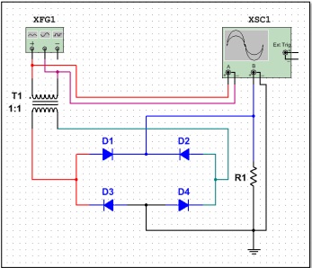
Figure 2.6 - Example of a full-wave rectifier circuit
1. Start with a clean, empty breadboard.
2. In this circuit, you will need:
• 4 x 1N4004 diodes
• 1 x 10 k? resistor
• 1 x 1:1 isolation transformer
• 1 x Function generator
• 1 x Oscilloscope (2 channels)
3. In this section, you will be using both sets of power rails that run along the outside of the breadboard. Begin by connecting the function generator to one set of power rails.
4. The 1:1 isolation transformer has 6 terminals: 3 on one side, and 3 on the other. Insert this into the breadboard such that none of the terminals are connected. A good place is in the middle of the breadboard, much like you can do with an IC.
5. Connect one of the end terminals of the transformer to the positive lead of the function generator, the other end terminal on that side to the negative lead, and the middle terminal will remain disconnected.
6. Change the parameters on the function generator so that it is outputting a Sine wave with frequency of 50 Hz, amplitude of 5 VPP, offset of 0 VPP. Make sure that the OUTPUT is turned off.
7. On the other side of the transformer, connect the positive power terminal (the one directly across from the one you previously connected) to the other power rail, not to the one that the function generator is connected to. Similarly, connect the corresponding negative terminal to the remaining power rail.
8. Explain why you need an isolation transformer in this circuit (hint - Oscilloscope ground pins are internally connected)
9. Connect the transformers positive power rail to one diode that is in forward bias and to another that is in reverse bias. You should have two diodes in parallel.
10. Connect the diode that is in forward bias to another diode that is in reverse bias, making two diodes in series.
11. Connect the first reverse diode to the remaining diode that is in forward bias, creating another series pair of diodes.
12. Connect the outputs from both of the parallel diode circuits, that is the second forward bias and second reverse bias diodes, to the transformers negative power rail.
13. You should now have two pairs of series diodes in parallel with each other. One pair should have the stripes close to each other, and the other pair should have the stripes far away from each other.
14. Connect a 10 k? resistor so that one lead is connected to the junction between the first two diodes that are in series (positive rail > forward > reverse > negative rail) and the other lead is connected to the junction of the other two diodes that are in series (positive rail > reverse > forward > negative rail).
15. You now need to connect the first channel of the oscilloscope so that you are measuring the output of the function generator (on the function generator side of the transformer, NOT the isolated side).
16. Similarly, the second channel needs to be connected so that you are measuring the voltage directly across the resistor.
17. Turn the OUTPUT of the function generator on.
18. Set the vertical axes on the oscilloscope so that they are both at 1.00 V, and the horizontal axis to 2.00 ms.
19. Move the cursor on the oscilloscope so that you are measuring the peak voltages of both channels. Save this waveform, put it in your report, and quantify the peak positive difference between the amplitude in the signals. Why is the difference not the same as that which you observed in Part 2a?
20. Is there a phase difference between the input and output waveforms? Why?
21. What is the frequency of the output waveform?
Part 2c Non-inverting amplifiers
Having previously simulated a non-inverting amplifier circuit, you will now be constructing and analysing that circuit in physical hardware.
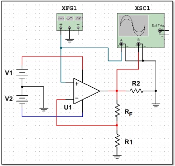
Figure 2.7 shows the Multisim circuit diagram for this section.
1. Start with a clean, empty breadboard.
2. In this circuit, you will need:
• 1 x LM358N operational amplifier IC
• 3 x 10 k? resistors
• 1 x 100 k? resistor
• 1 x Power supply (both channels)
• 1 x Function generator
• 1 x Oscilloscope (2 channels)
3. Just as you did for Part 3b, you are going to use the four power rails on the breadboard for different purposes. One rail will be GROUND; another will be the positive signal output from
the function generator; the third will be a negative power supply; and the last will be a positive power supply. Pay careful attention to which rail you are connecting to. The following instructions will reference these rails as above.
4. Start off by connecting the positive output of the function generator to one rail, and the ground connection to another rail. These now become your positive signal rail, and your GROUND rail, respectively.
5. Change the parameters on the function generator so that it is outputting a Sine wave with frequency of 50 Hz, amplitude of 2 VPP, offset of 0 VPP. Make sure that the OUTPUT is turned off.
6. Place the LM358N IC across the centre divider of the breadboard. Remember that ICs are static sensitive devices, so don't handle the IC more than necessary.
7. You now need to find the pin map for an LM358N operational amplifier. The datasheet for this component (or a similar manufacturer's equivalent) has been provided for you on LearnOnline, or you can refer to the internet. For the resource that is on LearnOnline, the information that you are after is on Page 3, where we are using an 8-pin DIP package, shown in the top figure. Additional information on the pin functions is shown in a table on the bottom of the same page.
8. The LM358N is a dual-operational amplifier package, but in this practical you will only be using the ‘A' amplifier.
9. Connect the ‘OUTPUT A' pin to your GROUND rail through a 10 k? resistor, and also through two 10 k? resistors. You should now have two 10 k? resistors in series, which are in parallel with the first 10 k? resistor.
10. To set the feedback for this operational amplifier, take the output of the voltage divider that you just created and wire it to the ‘INVERTING INPUT A' pin of the operational amplifier.
11. The ‘NON-INVERTING INPUT A' pin now needs to be connected to the positive signal rail that you created earlier.
12. You have previously used the power supply as a positive power supply, i.e. from 0 V to 12 V. For this circuit to function correctly you require a dual-voltage supply, i.e. from -12 V to 12 V. Change the parameters on the power supply so that both channel 1 and channel 2 have 12.0 V outputs with 0.10 A current limits. Make sure that the OUTPUT is turned off.
13. To connect this to the circuit, begin by connecting the power supply's positive terminal of channel 2, and the negative terminal of channel 1, to your GROUND rail.
14. Now connect the negative terminal of channel 2 to one of the two remaining rails on your breadboard. This now becomes the negative power supply rail.
15. Finally, connect the positive terminal of channel 1 to the remaining power rail on the breadboard. This now becomes the positive power supply rail.
16. Connect the oscilloscope so that channel 1 is measuring the output of the function generator, and channel 2 is measuring the ‘OUTPUT A' pin of the operational amplifier.
17. Turn the OUTPUTs of both the function generator and the power supply on, and observe the waveform on the oscilloscope.
18. Similarly to the previous parts of this practical, the AUTO function on the oscilloscope doesn't produce waveforms that are easy to compare.
19. Set the horizontal axis scaling to 5.00 ms and both vertical axes to 500 mV.
20. Move the cursor on the oscilloscope so that one is measuring the peak positive voltages of both channels, and the other is measuring the peak negative voltage. Save this waveform, put it in your report, and quantify the differences between the amplitudes
21. Using the non-inverting operational amplifier formula, calculate the gain of this circuit. Does this match the difference you are seeing on the oscilloscope?
22. Is there a phase difference between the input and output waveforms? Why?
23. For each of the parameter combinations shown in Table 2.1, take a screen shot of the resultant waveforms on the oscilloscope, put these in your report, and report both the positive and negative peak voltages for each screen shot. Make sure that you scale the axes to get the most amount of information on the screen as possible. Using the instructions above, you have already completed combination 1
24. Are the output waveforms always pure sinusoids? Why?
Table 2.1 - Non-inverting amplifier parameter combinations
|
Combination
|
RF
|
R1
|
VIN
|
|
1
|
10 k?
|
10 k?
|
2 VPP
|
|
2
|
100 k?
|
10 k?
|
200 mVPP
|
|
3
|
10 k?
|
100 k?
|
2 VPP
|
|
4
|
10 k?
|
100 k?
|
16 VPP
|
Part 2d Non-inverting buffers
Having previously simulated a non-inverting buffer circuit, you will now be constructing and analysing that circuit in physical hardware.
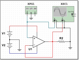
Figure 2.8 shows the Multisim circuit diagram for this section.
1. Due to the similarities with the previous circuit, use the existing circuit that is on the breadboard. Turn the OUTPUT of both the function generator and the power supply off.
2. Remove the voltage divider from the ‘OUTPUT A' pin of the operational amplifier, and i connect that pin directly to the ‘INVERTING INPUT A' pin.
3. Change the parameters on the function generator so that it is outputting a Sine wave with frequency of 50 Hz, amplitude of 2 VPP, offset of 0 VPP. Both channels of the power supply should be at 12.0 V and 0.1 A current limits.
4. Turn the OUTPUT of both the function generator and the power supply on and adjust the axes on the oscilloscope so that you can see at least two full periods of the waveforms. If you can't see one of the waveforms, set a small positional offset for one waveform only.
5. Is the amplitude of the output waveform the same as the amplitude of the input waveform? Why?
6. Is there a phase difference between the input and output waveforms? Why?
7. Using the non-inverting amplifier formula, show what the gain of this circuit is
Part 2e Inverting amplifiers
Having previously simulated an inverting amplifier circuit, you will now be constructing and analysing that circuit in physical hardware. Figure 2.9 shows the Multisim circuit diagram for this section.
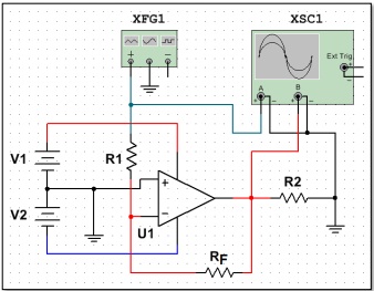
Figure 2.9 - Example of an inverting operational amplifier circuit
1. Due to the similarities with the previous circuit, use the existing circuit that is on the breadboard. Turn the OUTPUT of both the function generator and the power supply off.
2. Remove the connection between the ‘INVERTING INPUT A' pin and the ‘OUTPUT' pin. Also remove the connection between the ‘NON-INVERTING INPUT A' pin and the positive signal rail.
3. Change the parameters on the function generator so that it is outputting a Sine wave with frequency of 50 Hz, amplitude of 2 VPP, offset of 0 VPP. Both channels of the power supply should be at 12.0 V and 0.1 A current limits.
4. Connect the positive signal rail to the ‘INVERTING INPUT A' pin through a 10 k? resistor. Also connect the ‘OUTPUT' pin back to the ‘INVERTING INPUT A' pin through a 10 k? resistor.
5. Finally, connect the ‘NON-INVERTING INPUT A' pin through to your GROUND rail.
6. Make sure that channel 1 on your oscilloscope is measuring the input signal before the resistor.
7. Turn the OUTPUT of both the function generator and the power supply on and adjust the axes on your oscilloscope to suit.
8. For each of the parameter combinations shown in Table 2.2, take a screen shot of the resultant waveforms on the oscilloscope, put these in your report, and report both the positive and negative peak voltages for each screen shot. Make sure that you scale the axes to get the most amount of information on the screen as possible. Using the instructions above, you have already completed combination
9. Are the output waveforms always pure sinusoids? Why?
10. Is there a phase difference between the input and output waveforms? Why?
11. Why is there a ground reference between V1 and V2?
12. What would the output be in a square-wave was used instead of a sinusoidal?
Table 2.2 - Inverting amplifier parameter combinations
|
Combination
|
RF
|
R1
|
VIN
|
|
1
|
10 k?
|
10 k?
|
2 VPP
|
|
2
|
100 k?
|
10 k?
|
200 mVPP
|
|
3
|
10 k?
|
100 k?
|
2 VPP
|
|
4
|
10 k?
|
100 k?
|
16 VPP
|
Part 2f Comparators
Having previously simulated a comparator circuit, you will now be constructing and analysing that circuit in physical hardware. Figure 2.10 shows the Multisim circuit diagram for this section.
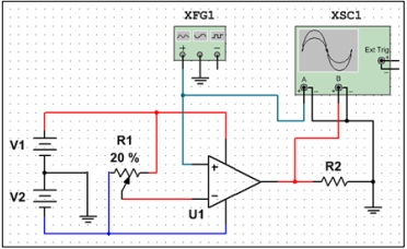
Figure 2.10 - Example of a comparator circuit
1. Due to the similarities with the previous circuit, use the existing circuit that is on the breadboard. Turn the OUTPUT of both the function generator and the power supply off.
2. Remove the connections from both the ‘INVERTING INPUT A' and ‘NON-INVERTING INPUT A' pins on the operational amplifier, and remove the two resistors that are now disconnected.
3. Change the parameters on the function generator so that it is outputting a Sine wave with frequency of 50 Hz, amplitude of 10 VPP, offset of 0 VPP.
4. Connect the ‘NON-INVERTING INPUT A' pin directly to the positive signal rail.
5. Insert a 10 k? potentiometer into the breadboard, taking care not to short the terminals.
6. In your previous practicals, you have used a potentiometer as a variable resistor (rheostat) to vary the resistance in a circuit. You will now be using the potentiometer in a more traditional manner, and that is to vary the voltage, or potential, of the circuit.
7. Connect one end terminal of the potentiometer to the positive power supply rail, the wiper to the ‘INVERTING INPUT A' pin, and the last end terminal to the negative power supply rail.
8. Channel 1 needs to be measuring the ‘INVERTING INPUT A' pin, channel 2 the ‘OUTPUT' pin, and channel 3 the ‘NON-INVERTING INPUT A' pin.
9. Turn the OUTPUT of both the function generator and the power supply on.
10. Change the horizontal axis scaling on the oscilloscope to 5.00 ms. Also change the vertical axis scaling so that channel 1 is at 2.00 V/division, channel 2 is at 5.00 V/division, and channel 3 is at 2.00 V/division.
11. Vary the potentiometer wiper position and observe what happens to the waveforms on the oscilloscope. Take two screen captures for two different wiper positions, put these in your report, and explain the operation of the circuit
12. Is there a phase difference between the input and output waveforms? Why?
3 Summary questions
The following sections pose some questions with regards to the design of diode or operational amplifier circuits.
Part 3a Diodes
1. Is there any functional difference between a diode and an LED?
2. If a DC source of 5 V was used for both the half-wave and full-wave rectifier circuits, what would the outputs be? Are they the same? Why?
3. What limits the current in both the half-wave and full-wave rectifier circuits? Does the amount of current flowing through the diode matter?
Part 3b Operational amplifiers
1. What is the limitation when designing operational amplifier circuits between the gain and the supply voltage?
2. What compromises are needed when deciding what operational amplifier configuration to use?
3. Why do we need to use a dual supply for the amplifier circuits? Could we use just a single supply for them? If so what would happen if you applied more voltage to the negative input than the positive in terms of the output?
Attachment:- Electricity and Electronics.rar