Reference no: EM132557764 , Length: 5 pages
Problem Set
Problems 1 - 10 are from the text reading. Problems 11 - 20 are from the lecture notes on computer architecture.
Q1. In a PC using an Intel 80x86 microprocessor, the number of bits in the EBX register is ______
Q2. In a PC using an Intel Pentium microprocessor, the number of bits in a physical memory address is ______
Q3. In a PC using an Intel Core 2 microprocessor, the number of bits in the RBP register is ______
Q4. In a PC using an Intel 8086, the number of bytes in a memory segment was ______
Q5. Suppose that the EAX register contains FFFFFFC8 and the instruction add eax, 211 is executed. What will be in the EAX register, and what will be the values of SF, ZF, CF and OF?
Q6. What is the name of the register in which 80x86 flags are stored?
Q7. Draw a diagram showing the relationship of the EDX, DX, DL and DH registers.Page 29 shows EAX that you can follow as a template.
Q8. Briefly explain the difference between a compiler and an interpreter.
Q9. Suppose that you buy a 64-bit PC with 8 GB of RAM. What is the 16-hex-digit of the "last" byte ofinstalled memory?
Q10. Explain the difference between flat memory and segmented memory.
For Problems 12 and 13, use the diagram of the adder below.
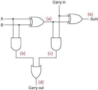
Q12. Suppose A = 0, B = 1, and Carry In = 0, show the values marked (a) thru (e) in the diagram above.
Q13. Suppose A = 1, B = 0, and Carry In = 1, show the values marked (a) thru (e) in the diagram above.
Q14. What is the benefit of the prefetch buffer the in the fetch-decode-execute cycle?
Q15. Use proper unit labeling in your solutions. Suppose you have the 5 stage pipeline shown here:
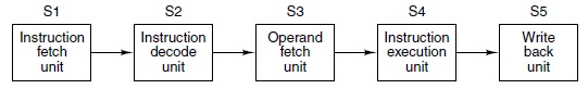
S1 takes 2 nsec to execute.
S2 takes 2 nsec to execute.
S3 takes 2 nsec to execute.
S4 takes at most 12 nsec to execute.
S5 takes 2 nsec to execute.
(a) What is the latency of a single instruction?
(b) What is the bandwidth (MIPS) of this pipeline?
(c) Briefly explain how a superscalare architecture can alleviate the bottleneck in S4.
(d) Suppose a superscalar architecture was implemented, and S4 decreased to 4 nsec. What is the latency of a single instruction?
(e) With S4 decreased to 4 nsec, what is the bandwidth (MIPS) of this pipeline?
Q16. Show how the hex bytes E6 34 0A 11 would look in little endian format in the following memory cell:
Q17. What does the program counter (EIP register in 80x86) point to?
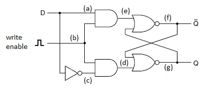
Q18. How are memory writes controlled in a clocked D-latch?
Q19. Suppose the clocked D-latch below is currently in a stable converged state of Q = 1.Now you want to write a 0 to the data line to change the state of the latch so that it stores a 0. Trace through the operation of the circuit, explaining the values of (a) through (g) in the process.
Q20. In the lecture, we showed a 4 bit memory using D flip-flops. There is a method of writing to memory registers using something called a shift register, where data is fed into each flip flop one bit at a time. The bits are shifted into the next flip-flop as the data is fed into the register. Here is an example where we are writing the bits 0110 into a 4-bit memory. The least significant bit is first fed into the "leftmost"flip-flop, and it is shifted through until all of the data is read into the register.
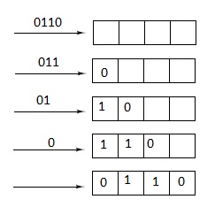
Design and draw a circuit for a 4-bit shift register comprised of D flip-flops.