Reference no: EM133121651
Digital Combination Locker
Objective
» Convert a word specification to a Finite State Machine
» Use the Synchronous Design Methodology to derive the VHDL code of the FSM
Specification
We want to design a 3-digit combination lock to allow entry to a locked room. The lock has a reset button, an enter button, and a 16-keypad on which the user can enter one value at a time on the input pin value. When the signal unlock is asserted, an electromechanical relay is released, allowing the door to open.
Operations
The unlock process begins when the operator presses reset. He or she then presses a key, followed by the enter button. This is repeated for the second and the third key digits. After entering the three 4-bit digits, the door will be unlocked or not depending on whether the sequence of key pressed was correct. We will use the following: 7,5,9 as the code sequence.
The process can be retried at any time simply by pressing reset again.
The figure below gives a block diagram of the entire combination lock consisting of the two principal components: data path and controller.
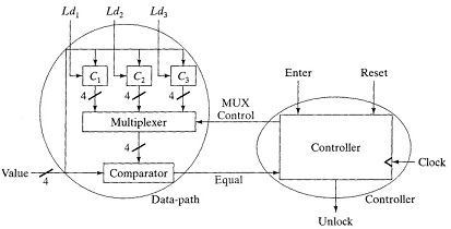
The data path operates on data values, and the controller keeps track of where we are in checking the combination. The data path component consists of the three registers (C1, C2, and C3), a multiplexer, and a comparator. The three registers hold the lock combination which is taken from same input pin value using the appropriate Ld, signal. One can use the keypad to enter a new value and assert a load signal to change a digit of the combination. Once the combination is entered, the controller which can be described as a finite state machine provides the appropriate value for the MUX control to select the appropriate value to be compared with the inputted value.
What needs to be done:
1. Translate the word specification of the controller to Moore finite state machine.
2. Write a synthesizable VHDL code for the entire design (Data Path + Controller). Use a multi-segment VHDL code for the FSM controller. For the datapath, you may also make use of combinational processes, concurrent signal assignment statements, clocked processes to infer the three register Cl, C2, and C3. Note that you should load the values 7,5,9 respectively.
3. Simulate your design with the Modelsim simulator to verify correct functioning for several typical values of the input.
Use the following design entity.
Library IEEE;
USE IEEE.std_logic_1164.all; ENTITY comb lock IS
PORT ( ldl : IN STD_LOGIC;
1d2 : IN STD_LOGIC;
1d3 : IN STD_LOGIC;
value : IN STD_LOGIC VECTOR(3 DOWNTO 0);
enter : IN STD_LOGIC; reset : IN STD_LOGIC; clock : IN STD_LOGIC; unlock : Out STD LOGIC);
END ENTITY;