Reference no: EM132112484
EXPERIMENT 1 - Fourier Analysis
Objective: Objective of this experiment is to perform Fourier analysis for a square wave and to extract fundamental and harmonics using band-pass filters.
Prelab:
1. Perform Fourier Series analysis on the following waveform v(t) and write down its equation.

Figure 1: Square Wave v(t)
2. For the following passive band-pass filter (figure 2), find out the parameters as required.

Figure 2: - band-pass filter
3. Design the band-pass filter in PSpice with v(t) as your input. Perform transient analysis and observe the waveform across R1, vR1. Draw a rough sketch of vR1 and explain its relationship to v1. Also, measure its amplitude, frequency and time period.
Lab Work:
1. Build the passive band-pass filter and provide v(t) as your input. Use oscilloscope to observe v(t) and vR1(t) simultaneously. Draw a rough sketch of the output vR1(t) and measure its amplitude, frequency and time period.
2. Change the value of capacitor in the filter, keeping inductor and resistance the same, to filter out the third harmonic. Draw a rough sketch of the output and measure its amplitude, frequency, and time period
EXERCISE:
Write a MATLAB program that asks user to enter the amplitude, time period, and number of harmonics required to calculate the Fourier series of a square waveform such as the one used in the lab. Plot the output v(t) from its Fourier series.
EXPERIMENT 2 - Diode Bridge Modula tor
Objective: Objective of this experiment is to create Diode Bridge Modulator circuit to study Double Sideband Suppressed carrier (DSB-SC) modulation and to perform modulation of a tone signal.
Prelab:
1. Basic idea behind Diode Bridge modulator is to create a switch using diodes that can switch the input message signal ON and OFF with the frequency of the carrier. This can be done using the following circuit
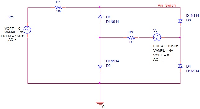
Figure 1: Diode Bridge Switching Circuit
Create diode bridge switching circuit shown in figure 1 in PSpice and perform transient analysis to observe the following output at node Vm_Switch. Write down the time-domain expression for the output in the space provided below.

Figure 2: Output of Diode Switch Circuit
2. Derive the expressions for the frequency spectra of vm and vm_switch(t) and write them down. Also, draw a rough sketch of the spectra.
3. Complete the modulating circuit to extract the component located at fc using a band-pass filter (tank circuit) to get DSB-SC modulated tone signal. Simulate it and observe voltage at vout and write down its peak-to-peak value.
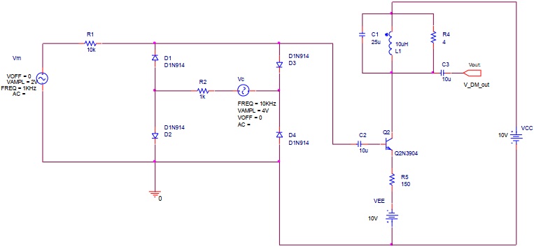
Figure 3: Diode Bridge Modulator
4. For the tank circuit (parallel band-pass filter), calculate the value of center frequency and bandwidth. Refer to your circuit analysis book to review parallel band-pass filters.
5. Output of the diode modulator can be increased using an amplifier, such as MOSFET common-source amplifier or BJT common-emitter amplifier. Let's use a MOSFET common source amplifier to produce some signal gain. Design the common-source amplifier as shown in the following figure.
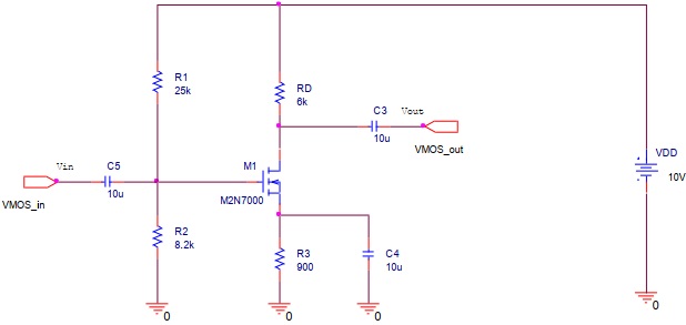
Figure 4: MOSFET Common-Source Amplifier with Input and Output DC Blocking Capacitors
6. Let's create sub-circuits for both the diode modulator and amplifier circuits so it will be easy to connect them together in a schematic page.
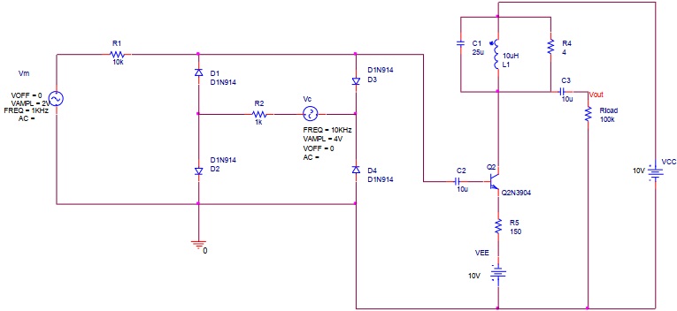
Figure 5: Diode Modulator Circuit with Hierarchical Port at the Output

Figure 6: Diode Modulator Sub-Circuit
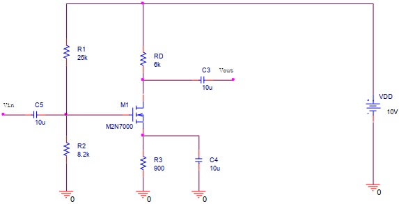
Figure 7: MOSFET Common-Source Amplifier with Input and Output Hierarchical Ports
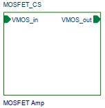
Figure 8: MOSFET Common-Source Amplifier Sub-Circuit
7. Connect Common Source amplifier at the output of Diode Modulator and observe the output voltage
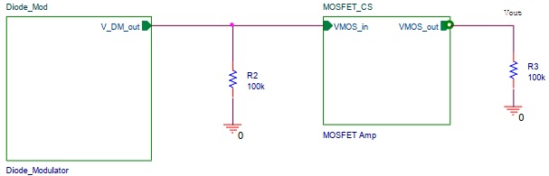
Figure 9: Diode Modulator Followed by MOSFET Common-Source Amplifier
Lab Work:
1. Build circuit from figure 1 and observe the output on the oscilloscope. Compare the observed waveform with the simulated one and explain if there is any difference.
2. Build circuit from figure 3 and observe the output on the oscilloscope. Compare the observed waveform with the simulated one and explain if there is any difference.
3. Build Common-Source amplifier as shown in figure 4 and test it with a 10mV, 1KHz sinusoidal waveform. Connect a 100K? load at the output. Measure the output of amplifier and calculate its gain.
4. Connect Common-Source amplifier at the output of diode modulator as shown in figure 9 and measure output of diode modulator and output of amplifier. Calculate gain of the amplifier again and compare it with the one calculated in step 3.
Lab Report Discussion:
Your discussion should include how does a diode bridge modulator work. Include proper equations to explain different parts of diode bridge modulator and discuss the differences between your simulated/theoretical and observed values, if any.
EXERCISE
Create a MATLAB program that asks user to enter four parameters,
(i) Frequency of the tone signal (fm)
(ii) Amplitude of the tone signal (Vm)
(iii) Frequency of the carrier (fc)
(iv) Amplitude of the carrier (Vc)
Based on the above information, calculate modulation index (μ) of the AM signal and print it in the command window. Also, plot three subplots with message signal, carrier signal and modulated signal. Properly label your subplots.
EXPERIMENT 3- AM Modulation a nd Demodulation
Objective: Objective of this experiment is to modify Diode Bridge Modulator circuit built in experiment # 2 into an AM modulator and to create an Envelope Detector that acts as an AM demodulator.
Prelab:
Simulate all of the circuits in PSpice. Perform theoretical derivations and calculations where required.
1. DSB-SC signal is basically an AM signal without any carrier. If a carrier is added into DSB- SC circuit, it can generate an AM signal. Create diode modulator circuit as shown in figure 1. Add hierarchical port (Place → Hierarchical Port → Portleft-L/CAPSYM) at the output as shown. Make sure to name your schematic and page to be the same.

Figure 9: Diode Modulator Followed by MOSFET Common-Source Amplifier
2. Next, create a summing amplifier (in a separate schematic/page) that will be used to add a carrier with the DSB signal produced by diode modulator. Add hierarchical input(place → Hierarchical Port → Portright-R/CAPSYM) and output(place → Hierarchical Port → Portleft-L/CAPSYM) ports as shown. Once again, your schematic and page should have the same name.
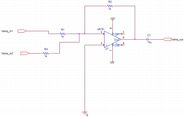
Figure 2: Op-Amp Summing Amplifier
3. Create MOSFET common-source amplifier (in a separate schematic/page) to be used to increase AM signal amplitude. Once again, add hierarchical input (place → Hierarchical Port → Portright-R/CAPSYM) and output (place → Hierarchical Port → Portleft- L/CAPSYM) ports as shown. Once again, your schematic and page should have the same name.
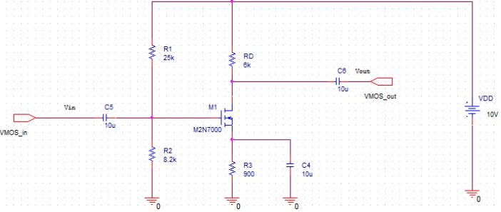
Figure 3: MOSFET Common-Source Amplifier
4. Calculate the amplifier gain (vout/vin) by adding a 100K resistor at the output and putting a 10mV sinusoidal source at the input (You have to remove the hierarchical ports first). Once you are done simulating the circuit for gain calculation, put the hierarchical ports back.
5. Create another schematic and make it root. Open a new page and name it to be the same as your schematic. Create the circuit shown in figure 4. Observe that three hierarchical blocks correspond to the three circuits designed earlier. On the circuit, draw rough theoretical sketches for the output of each of the sub-circuits and the final output of the circuit.

Figure 4: AM Modulator and Demodulator
Discussion:
Your discussion should include the description of each of the circuit module from theoretical point of view. Use mathematical equations to support your discussion. Compare your theoretical and practical results and suggest any improvements that can be made to make the circuit perform better.