Reference no: EM132227275
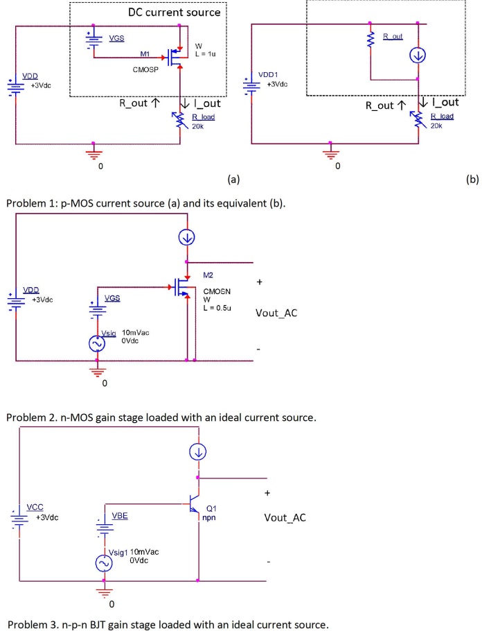
QUESTION 1
The p-MOSFET current source (see the schematic for Problem 1) operates with fixed gate-to-source voltage VGS =1 V. The circuit is powered from the DC voltage source VDD = +3V. The MOSFET design parameters are W=60 um and L = 1 um. Estimate output current value I_out in uA.
The MOSFET output resistance can be neglected.
The p-MOSFET is an enhancement-mode device fabricated with the following technology parameters: threshold voltage: Vtp = -0.8 V, process transconductance parameter: kp' = 70 uA/V2
QUESTION 2
The p-MOSFET current source (see the schematic for Problem 1) operates with a fixed gate-to-source voltage of 1 V. The circuit is powered from the DC voltage source VDD = +3V. The MOSFET design parameters are W =60 um and L=2 um.
Estimate the Output Resistance of the current source R_out in kOhm if the output current value is 100 uA.
The p-MOSFET is an enhancement-mode device fabricated with the standard technology parameters as follows: threshold voltage:
Vtp = - 0.8V, process transconductance parameter: kp' = 70 uA/V2, Early voltage parameter V'AP;= 10 V/um.
QUESTION 3
Estimate the required bias voltage VGS (an absolute value) for the p-MOSFET in the current source (see the schematic for Problem 1) to provide the output current value I_out = 40 uA. The MOSFET design parameters are W=50 um, L=0.8 um. Assume the standard process parameters as follows: k'p=70 uA/V2, Vtp= -0.8 V. The current source operates from VDD = +3V DC.
QUESTION 4
Estimate the maximum allowed output voltage for the p-MOS current source when the current value and the differential output resistance remain nearly constant, e.g. the mosfet operates in the saturation region.
The MOSFET is biased with the gate-to-source voltage 0.92 V (absolute value). The current source is powered from the DC voltage source VDD= +3V. Assume the standard process parameters: Vtp = -0.8 V.
QUESTION 5
The n-MOSFET gain stage (see the schematic for Problem 2) was biased with the gate-to-source voltage VGS = 1 V and loaded with an ideal current source. The MOSFET gate length was L = 0.6 um. The gate width was adjusted in accordance with the source current to keep the MOSFET in the saturation region. The process parameters were as follows: threshold voltage Vtn = 0.7 V and Early voltage parameter V'An = 20 V/um. Estimate voltage gain of the gain stage Av =Vout/Vsig (note that Vout and Vsig are amplitudes of AC signals).
QUESTION 6
The n-MOSFET gain stage (see the schematic for Problem 2) was biased with the gate-to-source voltage VGS = 1 V and loaded with an ideal current source with the output current value of 50 uA. The design parameters W and L were such that the MOSFET operated in the saturation region.
Estimate the MOSFET transconductance gm in mA/V.
QUESTION 7
In the n-MOSFET gain stage (see the schematic for Problem 2) the current source value was scaled up by a factor of 2 (doubled). The bias voltage VGS was adjusted accordingly to keep the MOSFET in the saturation mode. The design parameters W and L were NOT changed.
Evaluate the scaling factor for the AC voltage gain: estimate the ratio of the voltage gain values for the circuit with the scaled up current and for the original circuit.
Assume that the MOSFET was biased well above the threshold and operated with a large current.
QUESTION 8
Consider an npn BJT gain stage loaded with an ideal current source (see the schematic for Problem 3). The current source value was set to be 0.03 mA and the BJT bias VBE was adjusted accordingly to keep the BJT in the forward-active mode. The BJT Early voltage was VA= 35 V.
The circuit operated at room temperature T=300K (thermal voltage was VT = kBT/e= 26 mV). Estimate the BJT transconductance in mA/V.
QUESTION 9
Consider the same BJT gain stage shown in the schematic for Problem 3. The BJT has Early voltage of VA = 35V and the circuit operates at room temperature. Estimate the value of the voltage gain for AC signals.
QUESTION 10
The current source value in the BJT gain stage (see the schematic for Problem 3) was scaled up by a factor of 2 (doubled) and the VBE bias voltage was adjusted accordingly to keep the BJT in the forward active mode. Estimate the difference in the bias voltage values for the circuit after the change of the current and for the original circuit. The circuit operated at room temperature. Give an absolute value of the difference in Volts.