Reference no: EM132727357 , Length: word count:9000
Unit 19 Electrical and Electronic Principles - Higher National Certificate in Electrical and Electronics Engineering
Assignment - Electrical and Electronic Fundamentals
Learning Outcome 1: Apply an understanding of fundamental electrical quantities to evaluate circuits with constant voltages and currents.
Learning Outcome 2: Evaluate circuits with sinusoidal voltages and currents.
Learning Outcome 3: Describe the basis of semiconductor action, and its application to simple electronic devices.
Learning Outcome 4: Explain the difference between digital and analogue electronics, describing simple applications of each.
Assignment Brief
Scenario:
You are presented with the following tasks by the company where you train. The electric network company must carry out these tasks within a specified time limit and most importantly with the highest of standards and proficiency. To prove to the company that you are the right person to work for it you must carry out these tasks with utmost efficiency and professionalism and within the specified time limit. All the tasks involve solving AC and DC networks using the theory and practical experiences you acquired in your modules. All the tasks must be handed in one report which must be clearly and professionally presented.
Task 1
a. The circuit shown in figure 1.1 has the following element values: V= 12V, R1=2.2 kΩ, R2=1kΩ, R3=3.3kΩ. Apply Kirchhoff's voltage and current laws to analyse the circuit shown in figure 1.1 and determine the following:
i. The voltage across R1, R2,R3
ii. The currents in R1, R2 and R3
Iii. The total power dissipated in the circuit.
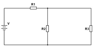
Figure 1.1 DC circuit series parallel
b. For the circuit shown in figure 1.2, the values of the resistors are: R1=15? , R2=10 ?, R3 =38 ? ; Determine the following:
i. The value of resistor Rx such that the total power dissipated in the circuit is 2.5 kw and
ii. The current flowing in each of the four resistors
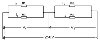
Figure 1.2 DC series parallel circuit with unknown Resistor
c. Determine the current flowing in RL in the circuit shown in figure 1.3 using Thevenin Theorem.
The values of the resistors in the circuit of figure 1.3 are as follows:
R1=40? , R2=60 ?, R3 =60 ? , R4 = 30 ? and RL=20 ?
and V= 30v
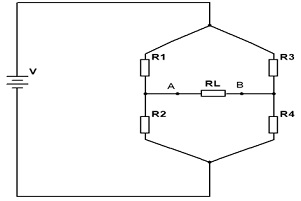
Figure 1.3 DC bridge circuit
d. Calculate the currents in the circuit of figure 1.4 ( where R1=12 ? , R2=3 ?, R3 =6 ? , V1=84 V and V2=21 V) using:
i. Superposition theorem
ii. Simulation software and
iii. Compare your simulated results with your analytical results.
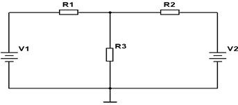
Figure 1.4 DC circuit with two voltage sources
Task 2
a. A series RLC circuit comprises an inductor of 80 mH, a resistor of 200 ? and a capacitor of 22 uF. If a sinusoidal current of 40mA at 50hz flows in the circuit of figure 2.1,
Analyse the operation of the circuit and determine :
i. Voltage dropped across the resistor
ii. Voltage dropped across the capacitor
iii. Voltage dropped across the inductor
iv. The impedance of the circuit
v. The supply voltage
vi. the phase angle
vii. Draw phasor diagram for the RLC series AC circuit in figure 2.1.
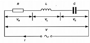
Figure 2.1 RLC series AC circuit
b. A coil of 3 k ? resistance and 0.12 H inductance is connected in parallel with a 0.02 µF capacitor across a 40 V, 5 kHz AC supply as shown in figure 2.2.
Analyse the operation of the circuit and determine the following:
I. The current in the coil
ii. The current in the capacitor.
Iii. Draw the phasor diagram and measure the supply current and its phase angle; and check the answer by calculation
iv. The circuit impedance
v. The power consumed
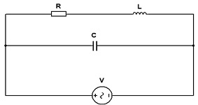
Figure 2.2 RLC parallel AC circuit
c. A coil of 1 k ? resistance and 0.1 H inductance is connected in parallel with a variable capacitor across a 2.0 V,10kHz AC supply as shown in figure 2.3.
Analyse the operation of the circuit and determine the following:
I. the capacitance of the capacitor when the supply current is a minimum
ii. The effective impedance ZT of the circuit at resonance.
Iii. The Q-factor
iv. The bandwidth
v. the current in each branch
vi. The supply current
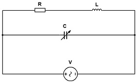
Figure 2.3 RLC parallel AC resonant circuit
Task 3
a. Describe the behaviour of a Diode, and draw its characteristics in terms of voltage and currents.
b. Demonstrate the action of the following semiconductor devices:
i. Diode (refer to figure 3.1(a) and (b) )
1. Measure and record the voltage and current across the diode for each entry in table 3.1 a and b.
2. Use the data of tables 3.1 a and b to draw the diode curve (V versus I)
3. Explain the diode curve from step 2
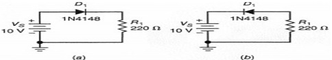
Figure 3.1 diode forward and reverse bias circuits
Table 3.1a forward bias
|
Vs
|
Measure VD
|
Measure ID
|
|
0
|
|
|
|
0.5
|
|
|
|
1
|
|
|
|
2
|
|
|
|
4
|
|
|
|
6
|
|
|
|
8
|
|
|
|
10
|
|
|
|
15
|
|
|
Table 3.1b reverse bias
ii. Zener diode (Refer to figure 3.2)
1. Measure and record the output voltages across zener diode for each entry in table 3.2
2. With the data in table 3.2, draw the reverse zener curve
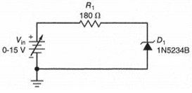
Figure 3.2 Zener diode circuit
Table 3.2 Data for Zener diode
|
Vin
|
Vout
|
Iz
|
|
0
|
|
|
|
2
|
|
|
|
4
|
|
|
|
6
|
|
|
|
8
|
|
|
|
10
|
|
|
|
12
|
|
|
|
14
|
|
|
iii. Bipolar Transistor as switch (refer to figure 3.3)
1. Measure VOUT when VIN = 0V and 10V and record the results in Table 6.1.
2. Measure IC and IB when VIN is 10V and record the results in Table 6.1.
3. Explain your results.
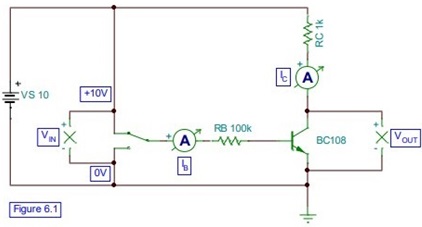
Figure 3.3 Bipolar transistor as switch
Table 3.3 Bipolar transistor voltage and current measurement
|
|
????????
when ?????? is 0??
|
????????
when ?????? is 10??
|
????
when ?????? is10??
|
????
when ?????? is 10??
|
|
measurement
|
|
|
|
|
c. Explain the operation of the diode in the full-wave bridge rectifier, the zener diode in a voltage stabiliser and the bipolar transistor as an amplifier.
d. Analyse the performance of Bipolar and FET transistors in terms of simple semiconductor theory, suggesting appropriate applications for each.
Task 4
a. Explain the difference between digital and analogue electronics. Illustrate your answer with examples.
b. Explain the amplifier characteristics in term of gain, bandwidth, input and output resistance and distortion level.
c. Explain the operation of the circuit in figure 4 and determine the Truth table for the following combinational logic gates circuit in figure 4.
d. Name the logic function of the combinational logic gate circuit in figure 4.
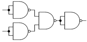
Figure 4 Logic circuit
e. Explain the benefits of using analogue and digital devices and circuits using examples
f. Evaluate the applications of analogue and digital electronics in Audio systems.
Attachment:- Electrical and Electronic Principles.rar