Reference no: EM132205153
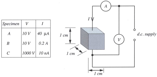
Question 1. In an experiment, the current through and the voltage across the opposite faces of three specimen blocks of material, each 1 cm3, was measured using the circuit of FIGURE 1. Use the results of the experiment, given in the table below, to classify each material as insulator, conductor or semiconductor.
Question 2. (i) Sketch and label energy-band diagrams of a metal, an insulator and a semiconductor and give approximate values of the energy gap where appropriate.
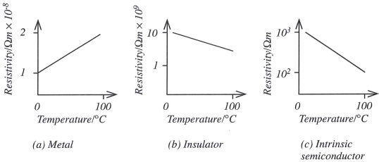
(ii) The three graphs of FIGURE 2 show how the resistivities of metals, insulators and intrinsic semiconductors vary over a small temperature range. Explain the shape of the graphs in terms of the energy-band theory of electrons in solids.
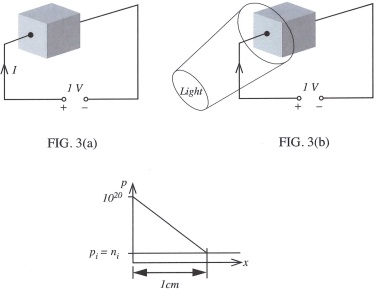
Question 3. (i) Determine the current flowing through a 1 cm cube of pure silicon when a potential of 1 V is applied across opposite faces (FIGURE 3(a)) if the number density of hole-electron pairs in the cube 1.56 x 10¹⁶ m-3.
(ii) A lamp is now allowed to shine upon one face of the cube as shown in FIGURE 3(b). This has the effect of generating hole-electron pairs at the surface of the exposed face and so raising the number densities of the carriers at that surface to a value of 1 x 10²⁰ carriers m-3.
For the polarities of external connections as shown, calculate the change in hole current due to the effects of the light.
NB. For the purposes of this question, we shall assume that the hole concentration p falls linearly with length x from 1020 m-3 down to its intrinsic value pi = ni at the opposite face, as shown in FIGURE 3(c). This would not be the case in practice; over such a long length, the density would fall exponentially.
(iii) If the polarity of the supply is now reversed, calculate the change in electron current due to the light. Again, assume a linear density gradient.
Question 4. (i) Use the Fermi-Dirac probability function
p(W)= (1+ expr(W -WF)/kT)-1 to calculate, for pure silicon at a temperature of 27°C, the probability of:
(a) an electron just being at the bottom of the conduction band
(b) a hole just being at the top of the valence band.
Question 5. A silicon 'chip' has the dimensions 8 x 2 x 2 mm.
(i) Calculate its resistance as measured between the square faces, assuming it is of intrinsic material. Take the carrier number density of hole-electron pairs as 1.5 x 10¹⁶ m-3 at room temperature.
(ii) Estimate its resistance at 10°C above room temperature.
(iii) Calculate the resistance, again across the square faces and at room temperature, if the 'chip' is now uniformly doped with aluminium, so that one in every 107 atoms is an impurity atom (a cubic metre of silicon contains about 5 x 1028 atoms). Also apply the 'law of mass action' to calculate the minority carrier density
(iv) Estimate the resistance of the doped 'chip' at 10°C above room temperature.
(v) Sketch, on the same axes, the energy/probability distribution curve for n-type silicon at two temperatures T1 and T2 (where T2 > T1) to show the effect of temperature upon the position of the Fermi level. (Hint: where would the Fermi level be if all the silicon atoms contributed a hole-electron pair?).
Attachment:- PHISIYCAL ELECTRONICS.rar