Reference no: EM13336163
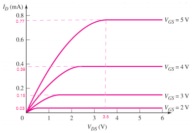
1- The transistor characteristics iD versus Vds for an NMOS device are shown in the figure below.
(a) Is this an enhancement-mode or depletion-mode device?
(b) Determine the values for Kn and VTN
(c) Determine iD(sat) for vGs = 3.5 V and vGs = 4.5 V.
2- The threshold voltage of each transistor in the figure below is VTn = 0.4V. Determine the region of operation of the transistor in each circuit.

3- The threshold voltage of each transistor in the figure below is VTp = -0.4V. Determine the region of operation of the transistor in each circuit.

4- The parameters of an n-channel enhancement-mode MOSFER are VTN = 0.5V, k'n = 120μA/v2, and W/L = 4. What is the maximum value of λ and the minimum value of VA such that for VGs = 2V, ro ≥ 200kΩ?
5- An enhancement-mode NMOS transistor has parameters VTNO = 0.8 V, γ = 0.8 V1/2, and Φf. = 0.35 V. At what value of VSB will the threshold voltage change by 2 V due to the body effect?
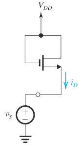
6- For the circuit in the figure below, sketch id versus vs for vs varying from 0 to VDD. Clearly label your sketch.
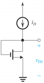
7- For the circuit in the figure below, find an expression for vDS in terms of iD. Sketch and clearly label a graph for vDS versus iD.
8- The PMOS transistor in the figure below has VTP = -0.5V. As the gate voltage vG is varied from +2.5 V to 0 V, the transistor moves through all of its three possible modes of operation. Specify the value of vG at which the device changes modes of operation.

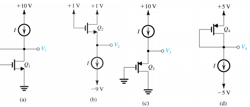
9- All the transistors in the circuits shown in the figure below have the same values of |VT|, k', W/L, and A. Moreover, A is negligibly small. All operate in saturation at ID = 1 and |VGS| = |VDS| = 3 V.
(a) Find the voltages V1, V2, V3, and V4.
(b) If |VT| = 1 V and 1 = 2 mA, how large a resistor can be inserted in series with each drain connection while maintaining saturation?
(c) If the current source 1 requires at least 2 V between its terminal to operate properly, what is the largest resistor that can be placed in series with each MOSFET source while ensuring saturated-mode operation of each transistor at ID = 1? In this limiting situation, what do VI, V2, V3, and V4 become?
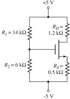
10- For the transistor in the circuit below, the parameters are VTN = 0.4 V k'n = 120 μA/V2 and W/L = 25. Determine VGS, ID, and VDs. Sketch the load line and plot the Q- point.
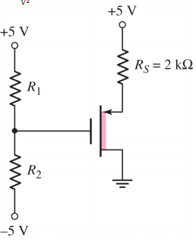
11- Design the circuit in the figure below so that VSD = 2.5 V. The current in the bias resistors should be no more than 10 percent of the drain current. The transistor parameters are VTP = 1.5 V and Kp, = 0.5 mA/v2
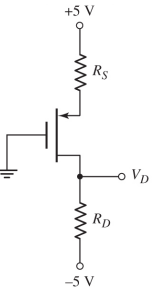
12- Consider the circuit in the figure below.
(a) Design the circuit such that IDQ = 0.25 mA and VD = -2 V. The nominal transistor parameters are VTP = -1.2 V, K'p, = 35 μA/V2 and viL = 15. Sketch the load line and plot the Q-point.
(b) Determine the maximum and minimum Q-point values if the tolerance of the k'p, parameter is ±5 percent.
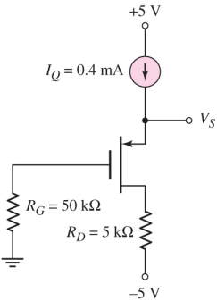
13-Consider the circuit in the figure below. The transistor parameters are VTP = -0.8 V, and KP = 200 μA/V2 Determine Vs and VSD.
14- The transistor in the circuit in the figure below is used to turn the LED on and off. The transistor parameters are VTN = 0.6 V, kn' = 80, and A = 0. The diode cut-in voltage is Vy = 1.6 V. Design RD and the transistor width-to-length ratio such that ID = 12 mA for V1 = 5 V and VDS = 0.15 V.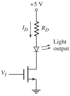
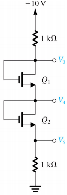
15- For the circuit shown in the figure below, find the labeled node voltages. The NMOS transistors have VTN = 1 V and k'n W/L = 2 mA/V2. Assume λ = 0.
