Reference no: EM132463316
ELEC S241F Electronic Circuit Design Assignment - The Open University of Hong Kong, Hong Kong
There are THREE sections in this assignment. You should answer all NINE (9) questions in this assignment.
SECTION A -
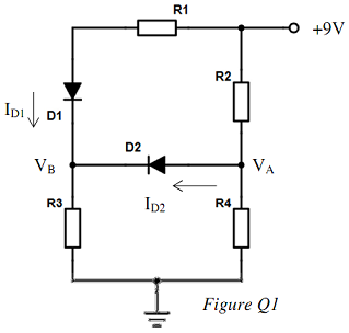
Question 1 - Consider the circuit in Figure Q1. Given R1 = 2 k?, R2 = 2 k?, R3 = 4 k?, R4 = 1 k?. The diodes D1 and D2 are assumed to have Vγ = 0.7 V.
(a) Assume that D1 is ON and D2 is OFF, determine the voltages VA, VB and current ID1.
(b) Use OrCAD to build the circuit in Figure Q1 to verify your answers in (a), i.e. find VA, VB and ID1.
Question 2 - Figure Q2 shows a NMOS common-source amplifier circuit. The NMOS transistor parameters are: VTN = +1.0 V, Kn = 0.5 mA/V2 and λ = 0. Given: VDD = +8 V, VGG = +2 V, RG = 3 k? and your RD.
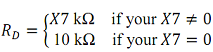
Remark: You must use your own RD to finish this assignment.
(a) Assume that the NMOS is biased in the saturation region. Find the Q-point parameters: IDQ, VGSQ, VDSQ.
(b) Show your assumption is correct.
Question 3 - A 6-bit digital-ramp A-D converter has a range of [0, +12V].
(a) What is the step size ? of this converter?
(b) State in binary form the final digital value that this A-D produces for an input voltage of +8.4V. Show all your calculations.
(c) Given the clock period is 1 µs, what is the maximum conversion time taken for this A-D converter?
Question 4 - A circuit is constructed from three flip-flops, as shown in Figure Q4, and outputs are taken from the Q output of each flip-flop. The initial values of these outputs are QA = 0, QB = 1, QC = 1 as shown. The flip-flops are all clocked from a common clock signal.
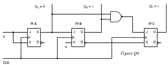
What will be the outputs after the receipt of four clock pulses?
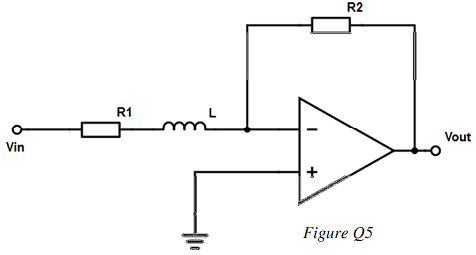
Question 5 - Consider the circuit in Figure Q5. Assume that the op amp is ideal.
(a) Using the phasor to prove that the voltage gain transfer function H(f) = Vout/Vin is given by
H(f) = - (R2/R1)/(1+j2πf(L/R1))
(b) How does H(f) change with frequency f increasing from 0 to infinity?
SECTION B -
Question 6 - A sequential machine will be designed to control the sequence of a lighting system. There will be two inputs A and B, and three outputs R, S and T. A state-transition diagram of this machine is shown in Figure Q6(a).
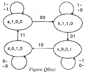
(a) In your answer book complete a copy of the state-table shown in Figure Q6(b) (attached).
(b) The partially completed state-assignment table for this system is shown in Figure Q6(c) (attached). The combination CD represents the present state and EF represents the next state, i.e. "state a" is assigned 00, "state b" 01 etc. In your answer construct a table which shows the input columns ABCD and has just the completed output columns for E, F and S.
(c) Use the Karnaugh map to find simplified Boolean expressions for R.
(d) Use two positive edge-triggered JK-type flip-flops (inputs J1 K1, J2, K2) to implement this sequential machine. Write down the Boolean expression for J1 K1, J2 and K2 in terms of A, B, C and D.
Question 7 -
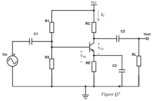
(a) Consider the BJT circuit in Figure Q7. Let R1 = 7 k?, R2 = 3 k?, Vcc = +10 V. Assume that VBE(on) = 0.7 V, β = 100, and VA = ∞. You can assume that the impedances of capacitors C1, C2 and C3 are negligible in the operating frequency.
Given the Q-point parameters are ICQ = 2.50 mA and VCEQ = 6.0 V.
(i) What is the operating mode of the BJT? Explain your answer.
(ii) Find the values of resistors RC and RE.
(b) Draw the small-signal equivalent circuit of Figure Q7.
(c) Find the small-signal voltage gain of the circuit.
(d) Use OrCAD to build the circuit as shown in Figure Q7. You can take vin = 1 mV, C1 = C2 = C3 = 100 µF, R1 = 7 k?, R2 = 3 k?, RL = 10 k? and your RC and RE in part (a)(ii).
Hint: You should use QbreakN in the breakout library to model your NPN transistor.
(i) Find the operating conditions of the circuit (i.e. the d.c. voltages at each node of the circuit). Print out both your schematics and output file.
(ii) Find the gain of the amplifier, i.e. Vout/Vin. Print out a plot of gain vs frequency over frequency 100 Hz to 1 MHz.
You must submit the schematic, output file and frequency plot of your simulation results in pdf format.
SECTION C -
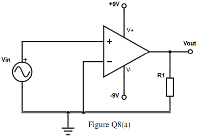
Question 8 - This question investigates the frequency response of a non-ideal op amp (uA741 in OrCAD) as shown in Figure Q8(a). You are going to find the open-loop low-frequency gain AO and open-loop (3dB) bandwidth fO of this non-ideal op amp using OrCAD.
Hint: You should use uA741 in the eval library to model your op amp.
The uA741 op amp has an open-loop voltage transfer function given by AV = Ao/(1+j(f/fO)).
Instructions:
1. Use OrCAD to build a circuit as shown in Figure Q8(b) (attached). Given Vin = 10 µV and R1 = 10 k?.
2. Create a new simulation profile. In the resulting Simulation Settings window, select AC Sweep/Noise as the analysis type and leave the options as General Settings. Set the Start Frequency to 1 and the End Frequency to 100meg.
3. Set the Point/Decade to 100. Leave the AC Sweep Type settings at Logarithmic and Decade. Save your setting and run the simulation.
You must submit both the schematic and output file of your simulation results in pdf format.
(a) Obtain a plot of the magnitude of gain |Vout/Vin| in dB vs frequency.
(b) Use cursor to find the open-loop low-frequency gain (in dB) from your plot. Find AO (not in dB).
(c) Use cursor to find the open-loop (3-dB) bandwidth fO.
(d) Find the gain-bandwidth of this op amp.
(e) (i) Use your own AO and fO to express AV.
(ii) Sketch the Bode plot of the magnitude of AV with frequency. On the sketch indicate the maximum magnitude of gain, any corner frequencies, and the values of any slopes. Use decibels for the gain scale and a logarithmic frequency scale covering the range 1 Hz to 10 MHz
Question 9 - The non-ideal op amp (uA741 in OrCAD) in Question 8 is used in a series-shunt feedback configuration (non-inverting amplifier) in Figure Q9. Given Vin = 1 mV, R2 = 20 k? and your own R1, where
(a) Use OrCAD to build the circuit in Figure Q9. You can refer to your simulation setting in Question 8. You should simulate the frequency response over the range 1 Hz to 100 MHz, with 100 points per decade for each gain setting.
(i) Obtain a plot of the magnitude of amplifier gain |Vout/V=| in dB.
(ii) Find the magnitude of the closed-loop gain ACL.
(iii) Find 3 dB bandwidth fCL for this non-inverting amplifier.
You must submit both the schematic and output file of your simulation results in pdf format.
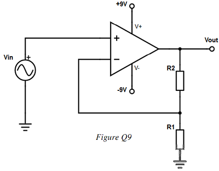
(b) Compute the voltage gain of this non-inverting amplifier in Figure Q9. Compare it with your simulated results in (a)(ii).
Attachment:- Electronic Circuit Design Assignment File.rar