Reference no: EM132599534
ELEC 20002 Industrial Electronics - Middle East College
Learning Outcome 1: Identify and analyze industrial electronic circuits;
Assignment Objective
Assignment will enable students to design, analyse and solve the problems. This assessment will develop their critical thinking, and problem solving skills.
Assignment Tasks
1) a. Calculate the output voltage ix and vo for circuit shown in figure 1.
Figure 1
b. Consider the instrumentation amplifier circuit as shown figure 2.
i. Derive the expression for the output voltage,vo with all necessary steps.
ii. Why do we keep RG, as variable resistor?
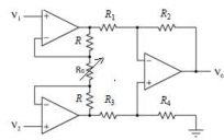
Figure 2
2) Design an op-amp circuit with resistors not less than 20 k? that will produce an output voltage of
Vout = (-20 dV3/dt - 15dV4/dt + 10V1 - ∫ 5V2)
[Use minimum number of op amps]
3) For a dual input unbalanced output differential amplifier configuration as shown in figure 3, determine the following by assuming that both transistors Q1 and Q2 are identical.
a. The collector to emitter voltage, VCE ,
b. Differential gain(Ad) and Common mode gain(Ac),
c. CMRR ;
d. Output if input voltages V1 = 90mV and V2 = 60mV for the CMRR value obtained from part c
e. If the input voltage V1 = 75m Sin (43982t) and V2 = 0mV . Draw the output waveforms obtained from V01 and V02 by showing clearly the amplitude and phase, corresponding to the input waveform. Take the differential gain obtained in part b for calculations. Assume that the common mode gain is zero.
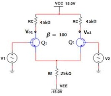
Figure 3
4) a. Suppose you want to determine the peak value of the waveform provided in figure 4. Design a suitable circuit and explain how it serves the purpose. [Note: You are expected to provide diagram, design calculations and operation of the circuit. Also required to draw the input and output waveforms clearly.]
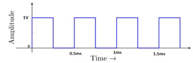
Figure 4
b. Consider an op amp with a slew rate of 2V/μs is working as an amplifier. The gain is given as 40dB.Calculate the maximum amplitude of the input signal ,so that this amplifier will faithfully amplify sinusoidal signals with frequencies from 0 to 30kHz without distortion.
ELEC 10002 Digital Logic Design
Learning Outcome 1. Perform experiments using logic circuits and build simple applications.
Learning Outcome 2. Demonstrate awareness to social responsibilities.
Assignment Objective
o Realise given Boolean expression using basic logic gates, simplify using De Morgan's laws and draw circuit for simplified Boolean expression
o Demonstrate universal property of NAND, NOR gates by realizing Boolean expressions using only NAND gates or only NOR gates
o To demonstrate the understanding of logic gates, give a basic logic gate circuit with 3 or 4 inputs and ask to find the output.
Assignment Tasks
Q1.
use De Morgan theorem to simply following expression
F = (A ¯ +C) ( A+ (AB) ¯ )
Draw the circuit after the De Morgan and verify the result in simulation program.
Complete the truth table 1 for the following SOP:
X= A ¯ BC +ABC ¯ +ABC +A ¯B ¯C ¯
Table 1
Q2.
For the logic circuit shown in Figure 1 write a Boolean expression for outputs X and Y.
Convert the Boolean expression for outputs X and Y into the standard SOP form and write a truth table.
Draw the output voltage waveform for the outputs X and Y. The applied input waveform at A, B and C inputs to the circuit are as shown in Figure 2.
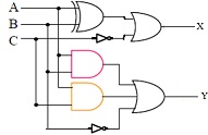
Figure 1
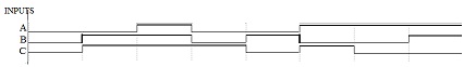
Figure 2
Q3.
Design a circuit that indicates whether a number between 0 through 15 is a prime number or not. The circuit must have four binary inputs A, B, C, D, and one output Y. The output signal y is true (Y =1) if the input represents a prime number and is false (Y=0) otherwise.
Construct a truth table to represent this problem
Derive the SOP of Y from the truth table.
Draw logic circuit for SOP .
Q4.
Implement an XOR gate using NAND gates alone and prove your design.
Convert the following Standard SOP to standard POS:
AB+ CD(AB ¯ + CD)