Reference no: EM132617649
ELEC 10002 Digital Logic Design - Middle East College
Learning Outcome 1: Differentiate the functions of the various logic gates using ICs and physical realization circuits.
Learning Outcome 2: Identify, illustrate, solve and simplify digital electronic problems switching algebra theorems and K maps.
Learning Outcome 3: Discuss various combinational logic circuits.
Learning Outcome 4: Discuss various sequential logic circuits.
Assignment Objective
o Design combentinal and sequentinal circuit.
o Simplify logic expression by using K map.
Assignment Task 1
a. Design a circuit to add two 2-bit binary numbers, and display the results of the addition as a 3-bit binary number, with the most significant bit be the carry out. Complete a truth table for the expected output. Use Karnaugh maps to simplify the Boolean functions for the outputs, and design realizations of the circuit using only NAND gates.
b. For the circuit shown in figure 1
i. Obtain the truth table for the logic circuit.
ii. Simplify the logic function using the K- map.
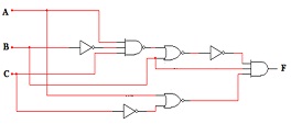
Figure 1
Q2
a. Simplify the following expressions using Boolean laws.
wy' + wx'y + wxyz + wxz'
b. Convert the following ( show all the steps):
i. (1101 1100 1101 1101) 2 to ( ) 10 to ( )BCD to ( )8
ii. (54097) 10 to ( ) 16
Q3 Design a 4-bit binary up counter circuit that counts the sequence from 0 to 15 and back to 0. Use Positive edge triggered D flip flop.
Q4
a. Complete the truth table and obtain the logic expression of the sequential circuit shown in figure 2 (show all steps).
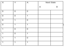
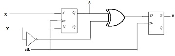
Figure 2
b. Convert SR Flip Flop to JK Flip Flop (show all the necessary steps).