Reference no: EM132463247
ECEN 454/ECEN 714 Digital Integrated Circuit Design Assignment - Texas A&M University, USA
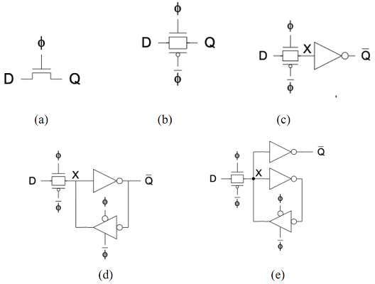
Question 1 - For the following latch designs from (a) to (e), additional transistors are added in each step. Explain what problem(s) was solved at each step?
Question 2 - For flip-flops, write down the relationship between clock frequency F, clock-to-Q delay Tcq, circuit delay Tp, setup time Tsetup, hold time Thold, and maximum clock skew Tskew. Assume contamination delay equals propagation delay.
Question 3 - Answer the following questions.
a. What does LVS stand for? What is the objective of LVS?
b. Draw a 6T SRAM bit cell. Specify the bit line and word line.
c. Draw a picture to show the difference between bonding wire vs flip-chip.
d. Draw an ESD protection circuit.
e. Explain electro-migration. What will happen in the end?
f. Give two methods to reduce dynamic power consumption.
g. Give two methods to reduce delay.
Question 4 - For the following layout, draw the circuit in gates.

Question 5 - Draw a transistor level pseudo-NMOS circuit of a (4-word)x(4-bit) ROM that stores the following information:
Word 0: 0110
Word 1: 1101
Word 2: 0111
Word 3: 1000