Reference no: EM133023516
Question 1
This question refers to a single-stage common source (CS) amplifier designed using the NMOSFET in question.
a. Draw a schematic showing the small-signal AC equivalent circuit of the CS amplifier with all components clearly labelled .
b. Determine the required load resistance RL to achieve the target Av.
c. Calculate the high-frequency cutoff, fH of the resulting CS amplifier.
d. Determine the VGS required to support the drain current.
about R_L. In this case, to achieve A_v, what is needed is a single resistor connected to the transistor near/at the output of the amplifier. I have generically refer to that as "R_L".
Question 2
This question refers to a cascode amplifier (CS-CG) designed using the NMOSFET in question.
a. Draw a schematic showing the small-signal AC equivalent circuit of the cascode amplifier with all components clearly labelled.
b. Determine the required load resistance RL to achieve the target.
c. Calculate the high-frequency cutoff, fH, of the resulting Cascode amplifier.
Question 3
For the cascode amplifier (CS-CG) in Question 2, express the frequency-dependent ABCD matrices (using the components of the small-signal equivalent circuit, for example, Cgs, Cgd, gm and s = jω to indicate frequency dependence) for
a. The CS stage
b. The CG stage
c. The CS-CG combination
d. Next, use MATLAB (or similar) to compute and plot the small-signal voltage gain |Av| of the cascode amplifier based on the ABCD parameters from 0.1 MHz to 10 GHz .
e. Finally, compare the 3 dB high frequency cutoff based on the calculation in Question 2 and the ABCD parameter method .
Question 4
This question again refers to the cascode amplifier (CS-CG) in Questions 2 and 3.
a. DC bias circuit design.
Design a bias circuit based on the schematic shown below.
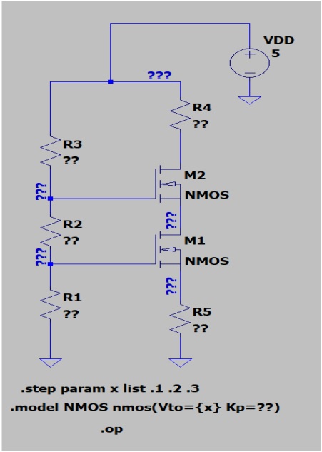
Constraints:
• R4 must be the same as the |Av| to achieve the target in Questions 2 and 3.
• VDD - 5 V must not change.
• The circuit topology must not be altered, for example, do not alter the schematic and do not add or remove pay
Design target:
• Despite the threshold voltage variation from 0.1 V to 0.3 V as reflected by the ".step", the bias drain current must be within 60 mA ± 4 mA. Show this using LTspice. Please clearly show your answer and the evidence to support it.
b. Small-signal AC analysis Constraints:
• VDD - 5 V must not change.
• The circuit topology shown below must not be altered.
Plot the small-signal AC gain from 100 Hz to 10 GHz. Show that the small signi AC midband gain of 9.5 V/V ≤ |Av| ≤ 10.5 V/V is achieved despite the threshold voltage variation 1rom 0.1 V to 0.3 V. Show this using LTspice. Please clearly show your answer and the evidence to support it (for example, use cursors to read your plot).
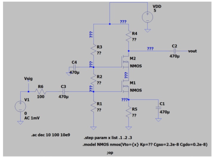
c. Finally, compare the high-frequency cutoff obtained from LTspice small signal AC analysis to the hand calculation and the ABCD parameter results.
Qustion 5:
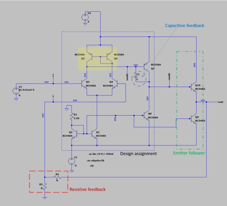
There are four components to this problem which we now review:
1. The dotted blue box refers to the circuit that was assigned in the Design Assignment. Note that the connections highlighted in the Q5 and Q6 have been altered slightly so as to tidy up the schematic. Please make sure that this is reflected in your work.
2. The addition of Cl feedback capacitor connecting the collector and base of Q7 is new. Cl is used as a compensation capacitor for stability as we will point out later.
3. The addition of Q9 and Q10 forming an emitter follower is new. The reason for this addition to isolate the resistive feedback network from adversely affecting the operation of the Op-amp.
4. The addition of R2 and R3 forming an external resistive feedback is new. Parts 1, 2, and 3 form a simple Op-amp as we depict in Fig. Q5b below.
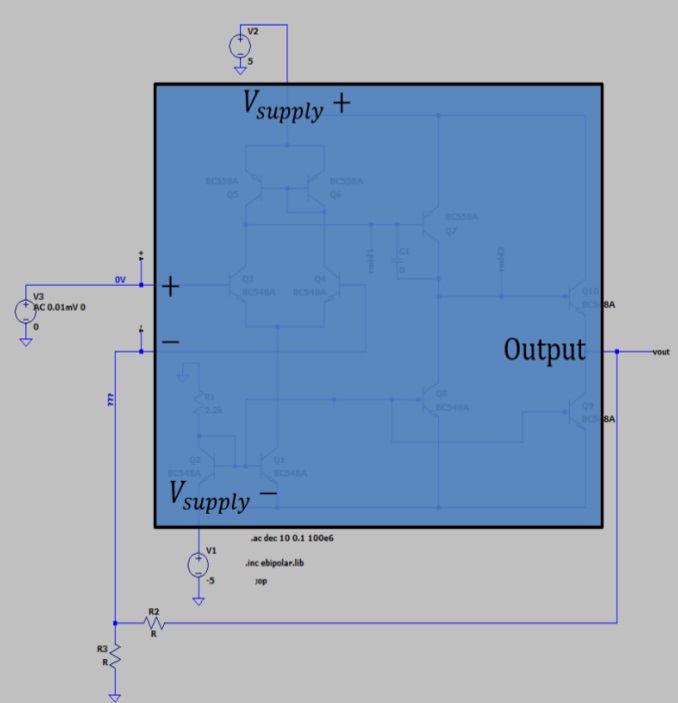
Opamp behaviour
a. How many poles does this open- loop Op-amp have and where are they (or is it) located in frequency?
b. If we desire no less than 45" phase margin for feedback amplifier using this Op-amp (as is), what is maximum allowable feedback factor?
Stability considerations for a noninverting amplifier using this Opamp.
c. Suppose we want to use this Op-amp (as is, with no compensation) to realize a non- inverting amplifier with a closed- loop gain of 10 dB, what is the appropriate ratio of R2/R3?
d. How much phase margin would we have? Is this phase margin adequate? What‘s the reason?
e. Plot the closed-loop gain of the uncompensated non-inverting amplifier over frequency. Show that the 10 dB closed- loop gain is achieved. suggest using resistors in the range of values in the kohms to tens of kOh ms. How much excess gain peak do you see?
Compensation using the feedback capacitor
We want 45n phase margin for the 10 dB gain non- inverting amplifier in the previous section.
f. At which frequency should we place the low-frequency dominant pole?
g. To realize the dominant pole, we use the feedback capacitor C1. Determine the value C1 so as to achieve the low-frequency dominant pole at the frequency computed in the previous step. Hint: we can think of this pole as one due to the interaction between the Miller capacitance due to C1 and the Q7 amplifier which interacts with ther of Q7.