Reference no: EM132835500
EEE2103 Electronic Devices
Problem 1
. i) Determine the value of Vo, I1 and I2 for the network of Fig 1.
ii) Repeat part (i) if the diode on the right be was made of Si instead.
iii) Repeat part (i) if it was made of GaAs instead.
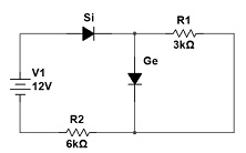
Fig.1
Problem 2
Task 1:
Apply the knowledge gained from Zener diode theories to construct a voltage regulator circuit which satisfies the following conditions. Please justify your choice of circuit by explaining how your circuit works.
Design Criteria:
1) Voltage regulation needs to be provided for the load so that the output voltage is a constant (10 + 0.1 × ID) Vas long as input voltage Vi and load resistor RL values are kept within appropriate ranges. (For Task 1, students don't need to specify Vi or RL values.)
2) Only Zener diodes (choose right VZ) and resistors (choose any small value between 500Ω and 1kΩ) can be used to construct the network.
Task 2:
Compute the range of values for RL and IL when Zener diode is in the "on" state, given input voltage Vi is a constant (20 + 0.1 × ID) V. Maximum current rating for Zener diode is IZM = 15 mA.
Task 3:
Compute the range of values for Vi when Zener diode is in the "on" state, given load resistor RL is a constant (2k + 0.8 × ID) Ω. Maximum current rating for Zener diode is IZM = 15 mA.
Problem 3
Apply the knowledge gained from diode theories to construct a clamper circuit that will give the following output from the given input.Please justify your choice of circuit by explaining how your circuit works and mathematically showing the derivation of vo. Here Vx = ID V. [5]
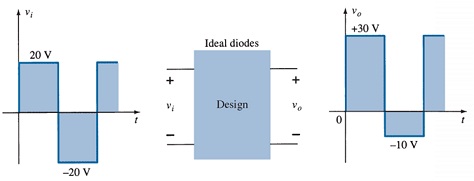
Fig.2
Problem 4
Consider the given output characteristics of a npnBJT employed in common-emitter configuration. Apply the knowledge gained from BJT theories to complete the following tasks.
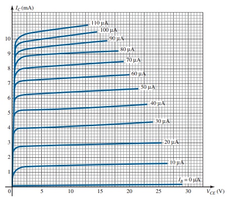
a. Draw a load line on the characteristics, given VCC = 25 V and RC = ( 2.5kΩ + ID × 100 Ω ) for a fixed-bias configuration. You must draw the load line on the graph given in page 4.
b. Label all the operating regions, and choose an operating point on the load line that is midway between cutoff and saturation.
c. Observe the value of IBon the operating point and calculate the RB value needed to get that IB.
d. What are the resulting values of ICQ and VCEQ?
e. What is the value of β at the operating point?
f. What is the value of α defined by the operating point?
g. What is the saturation current (ICsat) for the design?
h. Sketch the resulting fixed-bias configuration.
Attachment:- Electronic Devices.rar