Determine the small-signal voltage gain

Assignment Help Electrical Engineering
Reference no: EM132174502

Question 1: (a) A silicon dioxide gate insulator of an MOS transistor has a thickness of tox = 120 Å. (i) Calculate the ideal oxide breakdown voltage. (ii) If a safety factor of three is required, determine the maximum safe gate voltage that may be applied. (b) Repeat part (a) for an oxide thickness of fox = 200 Å.

Question 2: In a power MOS transistor, the maximum applied gate voltage is 24 V. If a safety factor of three is specified, determine the minimum thickness necessary for the silicon dioxide gate insulator.

Section - Transistor dc Analysis

Question 3: In the circuit in Figure P3.26, the transistor parameters are VTN = 0.8 V and Kn = 0.5 mA/V2. Calculate VGS, ID, and VDS
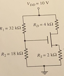
2391_3.26.jpg

Figure 3.26

Question 4: The transistor in the circuit in Figure P3.27 has parameters VTN = 0.8 V and Kn = 0.25 mA/V2. Sketch the load line and plot the Q-point for

(a) VDD = 4 V, RD = 1 kΩ and (b) VDD = 5 V, RD = 3 kΩ. What is the operating bias region for each condition?

866_figure3.jpg

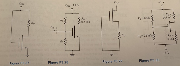
Question 5: The transistor in Figure P3.28 has parameters VTN = 0.4 V, kn' = 120 μA/V2, and W/L = 80. Design the circuit such that IQ = 0.8 mA and Rin = 200 kΩ.

Question 6: The transistor in the circuit in Figure P3.29 has parameters VTP = -0.8 V and Kp = 0.20 mA/V2. Sketch the load line and plot the Q-point for
(a) VDD = 3.5 V, RD = 1.2 kΩ and (b) VDD = 5 V, RD = 4kΩ. What is the operating bias region for each condition?

Question 7: Consider the circuit in Figure P3.30. The transistor parameters are VT? = -0.8 V and Kp = 0.5 mA/V2. Determine ID,VsG, and VSD.

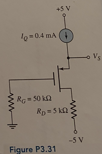
Question 8: For the circuit in Figure P3.31, the transistor parameters are VTP = -0.8 V and Kp = 200 μA/V2. Determine Vs and VSD

426_figure3.31.png

Question 9: Design a MOSFET circuit in the configuration shown in Figure P3.26. The transistor parameters are VTN = 0.4 V and k'n = 120 μA/V2, and RD = 5kΩ. The circuit parameters are VDD = 3.3 V and RD = 5 kΩ. Design the circuit so that VDSQ ≅ 1.6 V and the voltage across Rs is approximately 0.8 V. Set VGS = 0.8 V. The current through the bias resistors is to be approximately 5 percent of the drain current.

Question 10: Consider the circuit shown in Figure P3.33 The transistor parameters are VTN = 0.4 V and k'n = 120 μA/V2. The voltage drop across Rs is to be 0.20V. Design the transistor W/L ratio such that VDS = VDS (sat) + 0.4 V, and determine R1 and R2 such that Rin = 200kΩ.

187_figure3.34.jpg

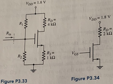
Question 11: The transistor parameters for the transistor in Figure P3.34 are VTN = 0.4 V, kn' = 120 μ,A/V2, and W /L = 50.

(a) Determine VGs such that ID = 0.35 mA. (b) Determine VDS and VDS (sat).

Question 12: For the transistor in the circuit in Figure P3.35, the parameter are VTN = 0.4 V, k'n = 120 μA/V2, and W/L = 25. Determine VGS, VDS. Sketch the load line and plot the Q -point.

Question 13: Design a MOSFET circuit with the configuration shown in Figure. The transistor parameters are VTp = -0.6 V, kp' = 50 μ A/V2, and λ = 0. The circuit bias is ±3 V, the drain current is to be 0.2 mA, the drain to source voltage is to be approximately 3 V, and the voltage across RS is to be approximately equal to VSG. In addition, the current through the bias resistors is to be no more than 10 percent of the drain current. (Hint choose a reasonable value of width-to-length ratio for the transistor)

Question 14: The transistor in the common-source amplifier in Figure P4.20 has parameters VTN = 0.8 V, k'n = 100 μA/V2, W/L = 50, and λ = 0.02 v-1. The circuit parameters are V+ = 5 V, V- = -5 V, IQ = 0 5 mA, and RD = 6 kΩ.

(a) Determine VGSQ and VDSQ.

(b) Find the small-signal voltage gain for RL = ∞.

(c) Repeat part (b) for RL = 20 kΩ.

(d) Repeat part (b) for RL = 6 kΩ.

637_figure4.20.jpg

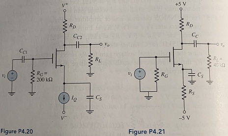
Question 15: The parameters of the MOSFET in the circuit shown in Figure P4.21 are VTN = 0.8 V, Kn = 0.85 mA/V2, and λ = 0.02 V-1. (a) Determine RS and RD such that IDQ = 0.1 mA and VDSQ = 5 5 V. (b) Find the small-signal transistor parameters. (c) Determine the small-signal voltage gain.

Verified Expert

In this assignment problems related to mos transistor were studied. The problems were of the numerical type and the related equations were used accordingly. The mos transistor biasing, the current-voltage characteristics and KVL are used.

Reference no: EM132174502

Questions Cloud

Research on a specific tool for strategic implementation : A brief description of your chosen tool, including relevant background, an APA-cited scholarly illustration, and detailed rationale for your choice
An analysis and description of the leadership styles : An analysis and description of the leadership styles and techniques used by the leader to help their team navigate through the situation
Generated using random number generation algorithm : Weights for the Prioritization Matrix are generated using a random number generation algorithm.
Distinguishing characteristics of good novels : One of the distinguishing characteristics of good novels is the ability of the writer to tell a good story while at the same time transcending time and place.
Determine the small-signal voltage gain : Determine VGs such that ID = 0.35 mA. (b) Determine VDS and VDS (sat) - Determine the small-signal voltage gain.
Control charts differ from run charts : Control charts differ from run charts in the following way:
Crossing two heterozygous individuals : What percent of the offspring will receive the recessive phenotype when crossing two heterozygous individuals? assume normal dominance.
What is the material most likely to be used in this type : What is the material most likely to be used in this type of weapons, and how might this type of weapon be deployed against an unsuspecting target?
What kind of legacy are you leaving : Reflect on your own personal attempts to balance your marriage, family, education, ministry, and leadership responsibilities. Do things need to change in order.

Reviews

Write a Review

Electrical Engineering Questions & Answers

  Determine the speed and slip of the machine

An AC induction machine has six poles and is designed for 60-Hz, 240-V (rms) operation. When the machine operates with 10 percent slip, it produces 60 N-m of torque.

  What gauge of wire would use if needed to limit power loss

You plan to integrate a sensor that operates at 24 VDC and 2A At distance of 100 feet from your controller under normal conditions. What gauge (AWG) of wire would you use if you needed to limit your power loss to 10%

  Find the required value of the filter capacitor

Specify the rms voltage that must appear across the transformer secondary. - Find the required value of the filter capacitor.

  Determine the a.c. resistance at 500 khz and at 10 mhz

At 1 kHz, the skin depth in copper is 2 mm. Determine the a.c. resistance at 500 kHz and at 10 MHz of 20 cm lengths of copper conductors having the following cross sections:

  Identify a particular lymph disorder

Identify a particular lymph disorder. Provide information on the disorders of the lymph system

  Determine the equation of motion of the system shown using

Determine the equation of motion of the system shown using Lagrange's method.

  Determine what are connected in parallel with the load

Three capacitors are found that each have an impedance of -j2.0, and they are connected in parallel with the load in a wye configuration. Determine the power factor of the combined load as seen by the source.

  What is the threshold level of this system

calculate the average signal-to-noise (SNR) in decibels (dB) Assume equal numbers of binary 0s and 1s.

  Determine the total power dissipated in the circuit

Determine the reference voltage VR. - Determine the logic 0 and logic 1 levels at the outputs vO1 and vO2. - Determine the total power dissipated in the circuit for A = B = logic 0 and for A = B = logic 1.

  Identify the interval of interest for performing convolution

Identify the intervals of interest for performing the convolution {x[n]*h[n]} on the following LTI system. This experiment requires that you write the summations for each interval of interest, but does not required you to simplify the summations.

  Design and simulate a power supply that takes line voltage

Design and simulate a power supply that takes line voltage(120v) and produces a 15V output with less than .5% ripple voltage with the following specifications use either full wave or full bridge wave.

  What synchronous reactance and armature resistance in ohms

A 100-MVA 11.5-kV 0.8-PF-lagging 50-Hz two-pole Y-connected synchronous generator has a per-unit synchronous reactance of 0.8 and a per-unit armature resistance of 0.012. What are its synchronous reactance and armature resistance in ohms?

Free Assignment Quote

Assured A++ Grade

Get guaranteed satisfaction & time on delivery in every assignment order you paid with us! We ensure premium quality solution document along with free turntin report!

All rights reserved! Copyrights ©2019-2020 ExpertsMind IT Educational Pvt Ltd