Reference no: EM132206373
Question 1. (a) FIGURE 1 shows a single-stage JFET amplifier circuit. The n-channel JFET has the ratings and characteristics given in the table below.
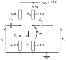
FIG. 1
(i) Show that the quiescent gate-to-source voltage is given by:
VGSQ = 2.57 - IDQRs
(ii) Determine the maximum quiescent drain current and drain-to-source voltage of the MET, using the 'square law' model of the device:
ID(SAT) = IDSS(1 - VGS/VP)2
(b) An LED works most consistently (giving a steady light output) if the current passing through it can be maintained constant, even if the supply voltage changes, for example, as the battery discharges over time. The circuit of FIGURE 2 shows a JFET being used as a constant source to drive an LED.
Determine a suitable value for Rs if the LED requires a constant current of 5 mA and the JEFT has an ipss value of 10 mA and a pinch of voltage of -3 V.
Question 2. (i) It is found that, when a MOSFET is operated in its saturation region, the drain current is related to the gate-to-source voltage by the equation:
ID = β/2 (VGS - VT)2
State upon which physical attributes of the transistor the value of β depends.
(ii) In comparing the behaviour of an n--channel MOSFET with a p-channel device having identical geometry and threshold voltage, it is found that the n-channel FET has a greater drain current than that of the p-channel FET. State why this should be so and give one other characteristic in which the two devices would differ.
(iii) FIGURE 3 shows a logic gate built from MOSFETs. Copy and complete the table and hence determine the type of logic gate.
FIG. 3
(iv) In order to increase the packing density, or the number of devices per unit area, that can be achieved on an integrated circuit, the supply voltage has been reduced. Very large scale integrated circuits (VLSI) now work at a 3.3 V supply or below.
Give two reasons why it has been necessary to reduce the supply voltage in order to achieve a higher packing density on the 'chip'.
Attachment:- TMA4.rar