Reference no: EM133351734
Question 1. Represent the operation of the simple switching circuits shown in FIGURE 1 by a truth table and by a Boolean expression.
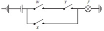
FIG. 1
Question 2. Simplify F = A‾B‾ (AV + B‾) using the rules of Boolean algebra.
Question 3. It was shown in Lesson 1 that the NAND gate can be used to derive all the other elementary logic operations (NOT, OR, AND). It is because of this feature that the NAND gate is called a universal logic gate.
Determine the elementary operations that can be derived from the
Exclusive-OR gate and hence establish if it a universal gate.
Question 4. (a) Construct the truth table for the function F given below.
(b) Use a K-map to minimise the function F.
(c) Sketch a logic circuit to realise the function F using only 2-input NAND gates.
(d) If the inputs A‾B‾C‾D‾ and ABCD are ‘don't care' conditions, use a K-map to derive the revised minimum expression for F.
F = A‾BCD‾ + AB‾C‾D‾ + A B‾C‾D + AB‾CD‾ + AB‾CD + ABC‾D‾ + ABC‾D + ABCD‾
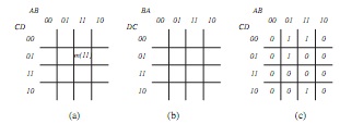
Question 5. The minterms of a truth table or K-map can be ascribed a number according to the binary weighting of the inputs. For example, in the map of FIGURE 2(a) and taking A as the least and D as the most significant bit, then cell row 2, column 3 is filled by the minterm having the binary weighting DCBA = 10112 and the cell's minterm can be represented by m(11).
(a) Complete the cell numbering for the entire map.
(b) K-maps can be constructed by arranging the input variables in various ways (there is no ‘right' way and depends upon the application and preference of the author).
Complete the cell numbering for the map of FIGURE 2(b).
(c) Present the map of FIGURE 2(c) in the format used in FIGURE 2(b).
Question 6. (a) Demonstrate by means of Boolean algebra that
A‾B‾ ⊕ C‾D‾ = (A + B) ⊕ (C + D)
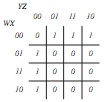
(b) Attempt to find the hidden Exclusive-OR hidden in the K-map of FIGURE 3 below.
Part 2
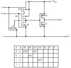
Question 1. (a) FIGURE 1(a) shows a logic gate built from MOSFETs. Copy and complete the table and hence determine the type of logic gate.
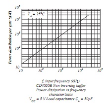
(b) FIGURE 1(b) shows the Power Dissipation vs Frequency characteristics of a CD4050B non-inverting Buffer gate. Briefly account for why the gate's power dissipation is frequency dependent.
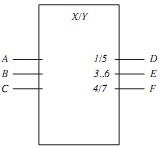
Question 2. Construct the truth table of the following coder:
Question 3. A logic circuit has three inputs and two outputs, FIGURE 3(a). The outputs are related to the inputs by the Boolean equations:
F1 = C‾B‾A‾ + CBA
F2 = C‾B‾ A + C‾BA‾ + CB‾A‾ + CBA
Show how the logic circuit can be realised using a dual ‘1-of-4' Data Selector/Multiplexer (e.g. LS153, FIGURE 3(b)) and a minimum of associated logic. Emulate and test your design using PSPICE.
[The LS153 can be found following the path:
Place/From model library/Digital MSI}
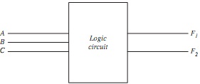
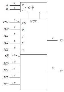
Fig 3
Question 4. Show the required fusing for PLA device of FIGURE 4 for it to form a single-bit full-adder.
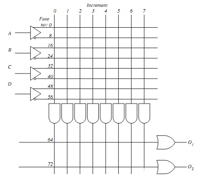
Fig. 4