Reference no: EM13852147
Problem #1

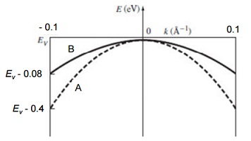
Two E versus k relations in the valence band for different holes each in two different materials (A, B) are approximated by the two different parabolas shown above. Note the units of k are Å-1.
a) Determine the effective mass of the two holes for both materials.
b) Which one has larger effective mass? What determines this?
c) Suppose that the E versus k relation in the conduction band for different electrons in each of the two materials is simply the mirror image of each of the parabolas shown. Would a hole in the conduction band for material B have positive or negative mass (be the same sign as your answer in part b)? Why or why not?
Problem #2
a) Calculate the temperature at which there is a 10-8 probability that an energy state 0.60 eV above the Fermi energy level is occupied by an electron.
b) Repeat part a) for a probability of 10-6.
c) Which of these occurs at a lower temperature? Does this make sense to you? Why or why not?
Problem #3
a) Plot the density of states in the valence band for silicon over the range of Ev ³ E ³ Ev - kT eV at 300K. You may use something like MATLAB if you like.
b) Determine the total number of energy states between Ev and Ev - kT eV for silicon at 300K.
Problem #4
Electrons in a particular material follow the Fermi-Dirac distribution function. At 300K, the Fermi energy for the material is 7.0 eV.
a) Find the probability of an energy level at 6.85 eV being occupied by an electron.
b) Repeat part a) for E = 7.15 eV at i) 300 K and at ii) 1000K. (You may assume that EF is a constant.)
Problem #5
Silicon is doped with 1015 /cm3 donor atoms and no acceptors atoms.
a) Plot the concentration of electrons versus temperature over the range 600K ³ T ³ 300K.
b) Calculate the temperature at which the electron concentration is equal to 1.1 x 10¹⁵ /cm3.
Problem #6
Determine the equilibrium electron and hole concentrations in GaAs for the following conditions:
a) T = 300 K, Nd = 1015 cm-3, Na = 4 x 1015 cm-3
b) T = 300 K, Nd = 3 x 1016 cm-3, Na = 0
c) T = 300 K, Nd = Na = 2 x 1015 cm-3
d) T = 450 K, Nd =1014 cm-3, Na= 0
e) T = 375 K, Nd = 0, Na = 4 x 1015 cm-3
Problem #7
For a particular silicon sample at 300K, boron impurity atoms at a concentration 1 x 10¹⁵ /cm3 are used to dope the material.
a) Determine the position of the Fermi level with respect to the valence band.
b) The Fermi energy is not where we would like it to be, so we want to add additional impurity atoms to move the Fermi level by kT towards Ev. Determine both i) the concentration; and ii) the type (acceptor or donor) of impurity atoms that need to be added. iii) Is the resulting material n or p type?
Problem #8
a) For silicon at 300K, if the semiconductor Fermi level lies 0.35 eV below the intrinsic Fermi level, find p0 and n0.
b) Assuming that p0 from part a) remains constant, determine the difference between the Fermi levels at T=400K and T=500K. Also find p0 and n0 at each temperature.