Reference no: EM13878410
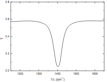
1. The optical transmittance T of a semiconductor wafer of thickness d is shown in Figure 1. Replicate this figure and draw the T- 1/λ curve where the semiconductor wafer is thinned, i.e. d is reduced. Justify your answer.
The reflectance remains the same:
T = (1-R)2e-ad)/(1-R)2e-2ad

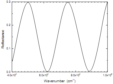
2. Light is incident perpendicular on a Si wafer covered with a dielectric of thickness d and refractive index n. The reflectance versus wavenumber is shown Figure 2.
Determine the dielectric thickness.
Where n= 2
And the following may be useful:
d = λ0λ1/2Π(λ1-λ0)

3. Consider an n-type wafer containing small n+ regions. A four-point probe is placed on the wafer so that probe 1 of a conventional in-line four-point probe is placed on one of the n+ regions. The other three probes are on the n-portion of the wafer.
In this four-point probe, current enters probe 1 and leaves probe 4; the voltage is measured across probes 2 and 3. There are no n+ regions between probes 2 and 4. Is the correct sheet resistance measured in this case? Explain your answer
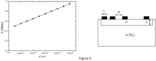
4. A transmission line measurement structure below gives RT values as shown in the graph (Figure 3). The doping density ND in the n+ layer is uniform.
Determine the sheet resistance RSH (ohms/square), the contact resistance RC (ohms) and the doping density ND (cm-3). Z (n+ layer width = 100µm, L= 25 µm, t = 2.5x10⁻⁴ cm, µn = 50 cm2/Vs).
