Reference no: EM132170977
Project: Part I (FSM Design Problem Part I-Section 2)
(b) Part II: Entire project
Goals
The goals of this project are:
1. To design a Moore FSM for performing the computation |A/5∫ for an n-bit number A, i.e., the integer quotient for A/5 .
2. To synthesize the FSM using the one-hot design style.
2 Part I: Design Problem (1500 points)
A digital circuit is needed that can compute |A/5∫ for an n-bit number A. However, since n can be large, due to pin limitations to the main circuit, only 2 bits of A can be fed at a time to it MSB first. Further, it was determined that a combinational circuit for |A/5∫ that has all n bits of A inputed to it in parallel cannot be afforded (the n bits could be shifted into a shift register 2 bits at a time, and after n/2 cc's (assuming n is even), all n bits will be available in parallel).
To meet the above constraints, one can design a finite state machine (FSM) to which each bit of A is fed sequentially, MSB first, on a bit-serial input line. However, it would then take at least n cc's to compute
|A/5∫. In order to speed up the computation by 2 x, 2 bits of A can be fed to the FSM (MSB first). So the requirement is to design an FSM with 2 bit-serial lines a1, a0 (a bit is fed on each line once every clock
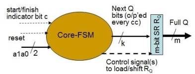
Figure 1: Possible schematic for the required required divide-by-5 circuit for an n-bit A. Note that m is related to the maximum n possible.
cycle) on which the bits of A are fed to it MSB first. The FSM needs to look at 2 bits of A at a time and determine the next quotient (Q) bits (Q = |A/5∫), what their place value position is, insert them in the right position in a register/shift-register RQ that will contain the final Q, and determine the next partial remainder Ri (remainder after the i'th iteration of computation, 1 ≤ i ≤ n/2, with R1 = 0). Note that Ri needs to be appended with the next bits on a1, a0 to form the next dividend Di = Ri|a1a0 to determine the next Q bits and Ri+1, and so forth.
Furthermore, n can be a varying number, and your FSM needs to determine Q = |A/5∫ and store it in RQ for any even n in the range [4, 16]. Thus a control signal c is also provided with a1, a0 that signals the start and end of A: for the all except the LS 2 bits of A c = 1, and c = 0 for the LS 2 bits. Thus whenever c goes from 0 to 1, it signifies that the MS 2 bits of A are on a1, a0 lines, and when c goes from 1 to 0, it signifies that the LS 2 bits of A are on a1, a0 lines. In between these two transitions on c, i.e., when c remains 1, the intermediate bits A are present on a1, a0 lines, each new pair of bits appearing every new cc. Thus using c, a new A can be fed to the FSM after the current A is processed. Finally, a reset signal is also provided that is activated only once and before any bits are fed to the FSM to reset it. After this, the FSM should go to the reset state on its own after it finishes processing the current A in order to wait for the new A A high-level schematic for the required system is shown in Fig. 1. Note that besides outputting the next bits of Q every clock cycle (cc), the FSM needs to also output control signal(s) to RQ so that they are stored in the right bit positions of RQ or end up in the right bit positions after the LS 2 bits of A are processed.
Note that in "regular" binary division, starting from the MSB of A, we consider only 1 bit of A at a time to determine 1 bit of Q at a time, and in the i'th iteration (1 ≤ i ≤ n), the dividend is Di = Ri|a0, where a0 is the next bit of A for the i'th iteration, i.e. the n - i'th bit of A. The division needed by your FSM is an extension of this process where the next 2 bits of A are processed in every iteration (there will thus be n/2 iterations) and a multi-bit Q and its bit positions need to be determined every iteration.
Hint: Determine what the FSM needs to remember (what different information classes), so that when it gets the current a1, a0 bits, it can determine the next Q bits and the next partial remainder.
Your submission should include the following.
1. Give a clearly labeled state transition diagram of the core Moore FSM needed in your design. Each state of the FSM should be labeled so as to understand the "meaning" of the state, i.e., what the state remembers about past inputs. There should be a clear indication of the reset state and an explanation why that state is correct to be the reset state.
2. Prove the correctness of your design. Essentially you need to prove: (a) the number of bits that you represent your partial remainder Ri in is correct, (b) the positions in the full Q of the next Q bits that you determine they belong to in each iteration is correct, and (c) that these positions do not overlap with the positions of the previous Q bits (otherwise, you'll need to perform some messy additions to obtain the correct Q). In order to prove these properties, try to prove them for regular binary division in which only 1 next bit of A, from MSB to LSB, is considered at a time. Then correctly (not by blind pattern matching) extend those arguments to the division that your design performs by looking at 2 bits of A at a time.
3. Synthesize the core FSM into a sequential circuit using one-hot state encoding (also called unary encoding) techniques using D FFs. Clearly draw this one-hot sequential circuit. Also show the control signal(s) to the register/shift-register RQ, and the connection of the system reset input to the FFs' set or reset inputs that forces the circuit into the reset state when the reset signal is active.
4. Assuming that a p-input gate has a delay of p units, analytically determine for an n-bit A, the delay of: a) the next-state logic unit of an FSM, and b) the output logic unit of an FSM as functions of n (if it happens that the delay of some unit(s) is a constant, i.e., independent of n, then that is fine). For this analysis, assume that n is a power of 2, say, 2k, and that k ≥ 4.
Based on the above delay components, analytically determine the delay of your circuit for computing |A/5∫ for an n-bit A. Assume that a D-flip-flop's delay and setup times are tff and tsu. 10% Writing down the final delay expressions is not enough; you need to derive them step by step.
5. Determine, also as a function of n, the combinational hardware cost of your circuit (i.e., cost of all components except FFs and registers) in terms of total gate inputs of the next-state and output logic
units of your FSMs.
Separately, also determine the number of D FFs (including those in registers/shift-registers) required in your design as a function of n.
3 Part II: Implementation and Simulation using Quartus II and Area Re- port from Design Vision (2500 points)
You are required to implement and simulate your design using the Quartus II CAD software as specified below:
1. The project is to be done in groups of 3. If you would like to to change your team to incorporate more or different team members as specified, please inform your current teammate right away and let the TA know your new team composition by Wed, 11/21.
2. Choose the schematic capture tool in Quartus to specify your design.
3. Device family to be used for the project is Max II which is selected by default in Quartus.
4. Please note the following two important issues for your design and its timing analysis:
• Keep your design as a "circuit" and do not make it a "chip". It seems that in the latter, the timing analyzer models the inputs and outputs of the circuit as i/o pins of a chip, which means they have a high capacitive load, and this messes the timing analysis of your design a bit. In any case, your design will be part of a chip, and thus should be kept as a circuit to get more realistic timing analysis for it.
• Note also that for performing timing analysis of your design you NEED TO set the Fitter setting in Quartus II to Standard Fit in order to get a more accurate critical path delays of your design.
5. Implement your design using D-FFs, registers, shift-register (SRs), (if not available, you can design shift registers easily using D-FFs and 2:1 Muxes), 2-input AND/OR/NAND/NOR/XOR/XNOR gates, NOT gates, 2:1 and 4:1 Muxes, 1:2 and 1:4 or 1:8 Demuxes, from the Quartus in-built library. How- ever, if any component (e.g., a shift-register, register, counter) does not have the necessary control signals for an FSM to control them, then you will need to design it yourself (as explained in class notes) using more basic components so that they have the required control inputs.
6. Design the basic next-state and output logic units using the above components, and simulate them for correctness (generate your own inputs for this simulation). Also perform static timing analysis (STA) to obtain the maximum delay of each combinational unit in the FSM. Provide this delay for this part. Note also that to determine the needed clock period (see below), the setup time of the FFs used in the FSM needs to be added to next-state logic delay, and the setup time of the register/shift-register used needs to be added to the output logic delay.
7. Based on the delays obtained in the above two items and the FFs' propagation delay and set-up times, determine a safe clock period Tclk = 1.1× (the maximum clock period needed) for each FSM implementation. Note that since your circuit is not a "placed" circuit (in which each component has a location, i.e., a 2-d coordinate value), and the clock is not routed, the simulator will assume an ideal clocking situation in which clock skew is zero, and this is also what you need to assume in determining Tclk. Show the Tclk derivation clearly.
8. Using the above designs and other in-built library components like positive-edge triggered D-FFs, obtain the one-hot FSM implementation. Provide schematics.
9. Using the above determined Tclk, simulate your entire design for all the input vectors (A's and any other control inputs) in the provided vwf file (you should also do your own simulations beforehand) and determine correctness, as well as delay as follows.
From the simulation, determine the absolute delay Tabs of your circuit in terms of real time units (i.e., not in terms of cc's but in terms of time units like ns's or ps's) as well as the cc delay Tcc, each as the max delay across all inputs. Time starts after the input A is stored in an input register/shift-register.
Provide relevant timing simulation waveforms (including showing the max-delay one) in your report.
Also clearly mention the number of correct outputs you obtain in your simulation both here and at the beginning of your report.
10. Conversion to VHDL and Area and Delay Reports from Synopsys's Design Vision:
First of all , please note you need to complete this Design Vision (DV) part to get points for the Quartus part, as the Quartus + DV portions form an integrated implementation and analysis portion..
(a) Convert your Quartus schematics to VHDL .
(b) Transfer the VHDL files to the ECE compute server in your directory for this project and use DV as explained in the tutorial session and documentation provided to you to compile the de-signs (synthesize the circuits) with all efforts set at the "medium" level. Provide all levels of schematics obtained after Design Compilation.
(c) Then collect only area reports (total area A1 and total cell area A2) for your design, and include the area reports verbatim in an Appendix at the end of your report (if too long, provide a relevant subset).
11. In a single table, provide the aforementioned Quartus delays (absolute and cc-based for the fsm-based design and the total DV-obtained areas (A1, A2's) and the A1 × (Tabs )2 metric.
Note that the (area)×(delay)2) metric means that we break even if going from one design to another we reduce area by a factor of k and increase delay by a factor of k. 35%
Important Note: Besides correctness of design, which is most important, you will be graded on the aforementioned metrics, especially A1 × (Tabs )2. These will be the main determinants of the grading of this item.
12. You need to submit a clearly written project report detailing all your work including all the steps and results of the design process (discussed in the previous section), use of the schematic capture tool, simulation results of component(s) and the final design, and other findings, if any, and conclusions.
The report should be professionally written using a text processing software (e.g., MS Word, latex), and all figures, plots, tables, etc. in it should also be generated preferably using some software tool. You should avoid hand-drawn/written material.