Reference no: EM132205162
Question 1. The measured 1-V characteristics of a silicon high-speed diode (BAS 16) are given in TABLE 1, below.
(i) Plot a graph of the diode's forward characteristic.
(ii) Compare the values of the diode's dynamic resistance and reverse current as obtained from TABLE 1 with those predicted by the diode equation. Attempt to account for any discrepencies.
|
VF
|
0.5
|
0.6
|
0.7
|
0.8
|
0.9
|
1.0
|
1.1
|
volts
|
|
IF
|
1.1
|
3.0
|
8.2
|
23
|
72
|
127
|
196
|
mA
|
|
VR
|
75
|
volts
|
|
|
IR
|
I
|
AA
|
TABLE 1 BAS16 Characteristics
Question 2. (a) Describe how 'depletion-layer'capacitance arises in a pn junction and identify three parameters that control its value. Give an application for a variable-capacitance diode.
(b) Question
In an experiment to determine the temperature dependence of the reverse saturation current, Is of a selected diode was measured at different temperatures. The results are given in TABLE B. The diode (1N4001) has an ideality factor of N = 1.90.
|
Temperature °C
|
Reverse current nA
|
|
20
|
16
|
|
25
|
26
|
|
30
|
33
|
|
35
|
53
|
|
40
|
73
|
|
45
|
106
|
TABLE B
Determine the value of the energy gap, %, and hence state the likely type of semiconductor used to make the diode.
[Hint: taking natural logs in equation (1) gives:
In(ls) = In (BT3/2) - WG/NkT
Over the small temperature span of the experiment the term In (BT 3/2) will not vary significantly and can be regarded as a constant.
Thus equation (2) is of the form y = mx + c. A graph of In(Is) against (1/7) will give a straight line of gradient m = - WG/Nk.]
Question 3. (a) Explain, with the aid of diagrams, the design features of a rectifier diode that enables it to have both a high current and high reverse-voltage rating. Your answer should make reference to device geometry, choice of materials and levels of doping. (Note that up-to-date information is available in manufacturers' data books and on the intemet.)
(b) A particular diode and its associated heat sink have the characteristics and ratings listed below. Calculate the maximum ambient temperature at which the diode can safely operate.
Diode
Maximum average forward current: /F(Av) = 20 A
Forward volt-drop (at IF(AV) = 20 A): 14 = 0.98 V
Maximum junction temperature: Ti = 200°C
Thermal resistance, junction to case: RTHj ease = 7 KW-I.
Heat sink
RTH = 0.5 KW-1.
(c) Explain how metal-to-semiconductor junctions may be ohmic or rectifying.
(d) Identify the properties of a Schottky type junction which give it applications in both low power integrated circuits and very high power discrete devices.
Question 4. FIGURE 1(a) shows a power supply using a full-wave bridge rectifier circuit. The mains supply is stepped down by the transformer T1 and the secondary voltage Vs rectified by the four diodes D1 -D4; diodes Dl and D3 conduct on one half cycle and D2 and D4 on the other. The diodes are provided in a single 4-pin bridge-rectifier package which can be mounted directly onto a printed circuit board.
The transformer has a turns ratio 10:1 and the average load resistance is 30 LI The output of the power supply is protected by a 3 A fuse which is designed to 'blow' within 5 ms if the current is in excess of ten times the rated value.
FIGURE 1(b) shows the voltage waveforms at various points in the circuit. Of interest here is the effect of switching on and off the mains supply; this has the effect of producing large transient voltages across the diodes.
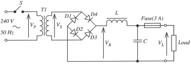
The switch is shown being closed at the worst case, at the peak of the supply voltage, and for this particular circuit it was found that the transient voltage being coupled to the secondary winding was up to 50% of the peak value of the primary voltage.
The worst time to re-open the switch, from a transient point of view, is as the primary voltage passes through zero, as, at this point, the rate of change of magnetizing current in the inductor is at its maximum (v = Lif) . The amplitude of the transient voltage produced across the secondary was found to be up to ten times its normal peak value.
Attachment:- SEMICONDUCTOR.rar