Reference no: EM132240183
Question 1: Design of LC Output Filter to Limit the Output Ripple Voltage of a filtered Rectifier Circuit.
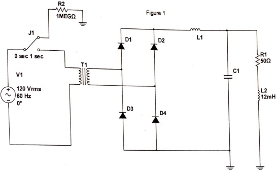
An LC Filter Shown in Figure 1 below is used to reduce the ripple content of the Output voltage for a single-Phase Rectifier. The Load resistance R1 is 50Ω, Load inductance L2 is 12mH and the frequency is 60Hz. The switched J1 is closed at time t=1 sec.
Step 1: Acquiring Your Individual Specification:
Record Your Specifications in the Spaces Provided Below
Vdc =
Ripple factor, ripple=
Ripple Voltage Vr=
Maximum Value of the Filtered Voltage, Vtmax =
Minimum Value of the Filtered Voltage, Vfmin=
Peak Value of the Rectified Signal, Vpeak
Turn Ratio of the Transformer =
Step 2: Design the Full-wave Bridge Rectifier and Filter Circuit show in Figure 1 below such that Your DC voltage and ripple factor meets the specification above. Note that the Frequency of the of the Input Voltage V1 is 60Hz. Assuming the effect of the Load is negligible, Carefully design for the Values of C1 and L1 so that your Specifications are met. Show your calculations below.
C1:
L1:
Step 3: Simulation of The Power Rectifier with Capacitive Filter: Using Multisim or PSPICE, setup the Circuit in Figure 1. To avoid a convergence problem due to a zero-Resistance path formed by R1 and C1 choose a small R1 Value of 100mΩ Simulate the circuit, plotting the current through the load inductor L2 and R2 and the Voltage across L2 and C2. Print these results over 5 Periods after steady-state.
Step 4: Describe the quality of the Rectification and LC filter by using the results of the simulation from Multisim or Spice to calculate the following parameters
(a) Average value of the Output dc Voltage
(b) Average value of the Output dc current
(c) Output dc power
(d) Root-mean-square of value of the output voltage
(e) Root-mean-square of value of the output current.
(f) Rectification Ratio
(g) Form Factor
(h) Ripple Factor
(i) Crest Factor
(j) Transformer utilization Factor
Figure 2 is a power diode with switched RLC circuit, and Figure 4 is a switched RL circuit with a freewheeling diode. For each of the Circuit, (a) Perform a Mathematical Analysis, to calculate the current through the resistor, using an initial condition of i(0) = 0 and assuming that the switched is closed at zero seconds and allowed to stay closed for 2 seconds. (b)Use Multisim or Pspice to simulate the circuit and perform a transient analysis of the circuits until the current reaches steady-state. And Print plots of the inductor voltage and current for each circuit. After the switch has been closed for some time, open the switch in Figure 4 and plot the inductor voltage and Current.
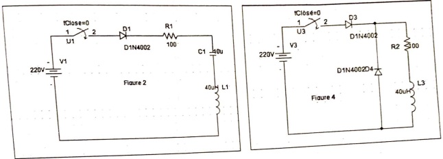
a) Analytical Solution to Figure 2.
b) Analytical Solution to Figure 4.
c) in Figure 2, change the inductor Value to 250 uH and simulate the circuit. Print your result for the inductor Voltages and Currents. Change the inductor value to 400uH and repeat the steps. Explain the differences in the result as your Inductor value changes from 220uH, 250uH and 400uH.
d) Analytical Solution to Figure 4 if the switch is opened at t= 2 Seconds after it has been closed for some time
d) Comment on the Results of Figure 4 when the switch is opened at t=2 seconds after it has been closed for some time.
e) Print a copy of each schematic, each plot and attach it sequentially.
Q3) The Bipolar Junction Transistor in Figure 5 is biased and configured to act as a switch. The BJT is specified to have a forced forward current gain in the range of 10 to 50. If VcE,sat= 1.0V and VBE,sat = 2V. Calculate the following
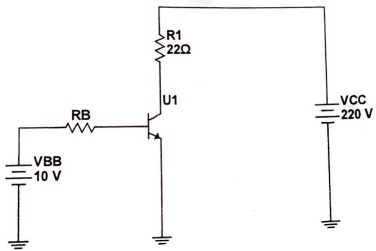
(a) the value of RB that forces the Transistor into Saturation with an Overdrive Factor, ODF of 10.
(b) The forced Forward current gain of bf
(c) Calculate the Power loss in the circuit
Attachment:- power electronics.rar