Reference no: EM132930953
ELEC4720 Programmable Logic Design - The University of Newcastle
ASSIGNMENT 1
Problem 1. Design a structural System Verilog module for a 7 segment display decoder with a four-bit input C, and a seven bit output Y , which can be used to display the character associated with the hexadecimal code represented by C on a 7-segment display on the development board. Instantiate your seven segment decoder module on the development board, and connect it with the switches and the seven segment displays to verify its functionality. To design the structural module you are required to carry out Boolean simplification, e.g., by using Karnaugh maps.
Marking Criteria: The circuit must be fully functional to get 5/5. For partially functional circuit your mark will depend on the results achieved.
Problem 2. Write a system verilog module to multiply two 4 bit wide numbers to produce a 7 bit wide result of multiplication. Create a test circuit on the development board to demonstrate the multiplier module is working properly.
Hint: Recall that the 7 bit wide product c of two 4 bit wide signals a and b can be calculated as
|
|
0
|
|
0
|
|
|
0
|
|
(a[3]
|
&
|
b[0])
|
(a[2]
|
&
|
b[0])
|
(a[1]
|
&
|
b[0])
|
(a[0]
|
& b[0])
|
|
+
|
0
|
|
0
|
|
(a[3]
|
&
|
b[1])
|
(a[2]
|
&
|
b[1])
|
(a[1]
|
&
|
b[1])
|
(a[0]
|
&
|
b[1])
|
|
0
|
|
+
|
0
|
|
(a[3] &
|
b[2])
|
(a[2]
|
&
|
b[2])
|
(a[1]
|
&
|
b[2])
|
(a[0]
|
&
|
b[2])
|
|
0
|
|
|
0
|
|
+
|
(a[3] &
|
b[3])
|
(a[2] &
|
b[3])
|
(a[1]
|
&
|
b[3])
|
(a[0]
|
&
|
b[3])
|
|
0
|
|
|
0
|
|
|
0
|
|
c[6]
|
c[5]
|
c[4]
|
c[3]
|
c[2]
|
c[1]
|
c[0]
|
Marking Criteria:
• Functionality (8) - To get 8/8 you must ensure that the multiplier is working properly.
• User interface (4) - To get 4/4 you must ensure that your test circuit is easy and intuitive to use.
Problem 3. Write that system verilog module to multiply two 8 bit wide numbers to produce the 15 bit wide result of multiplication. Design an appropriate testbench to test your multiplier module, and run the testbench in Modelsim to verify that the multiplier module produces correct results.
Marking Criteria:
• Functionality (8) - To get 8/8 you must ensure that the multiplier is working properly.
• User interface (4) - To get 4/4 you must ensure that your testbench is easy and intuitive to use.
Problem 4. In this assignment you will design the ‘logic unit' of the MIPS processor. This unit has one control unit F and two data inputs A and B. F is 2 bit wide. Each of A and B are 2n bit wide, where n is an integer. Typically n > 2, but that is not important for this assignment. The output Y is also 2n bit wide. The relation between the inputs and outputs is given in Table4.
| F [1:0] |
Y |
| 0 |
A & B (AND) |
| 1 |
A|B (OR) |
| 10 |
A ⊕ B (XOR) |
| 11 |
(A|B) (NOR) |
Table 1: Truth table for the MIPS compatible logic unit.
(a) Design an appropriate parameterized ( n is the flexible parameter) system verilog module to implement the logic unit. (b)(0.5 mark) Design an appropriate top-level module to test the circuit on the development board.
Hint: Use bit-wise operators to implement the logic operations. Then use a 4:1 MUX to select the output of the logic operation chosen by
F to be routed to the output.
Marking criteria: The mark for part (a) depends on the extent to which your circuit is able to meet the specifications. If it satisfies all the requirements, then you will get full marks. If it meets a subset of the specifications then the marks will depend on the results achieved.
The part (b) mark will depend on how user-friendly and complete your test methodology is.
Problem 5. Use the ‘+' operator in System Verilog to implement a parameterized 2n bit adder so that we can freely vary n during instantiation.
Next you will use the above adder module to build a circuit that will either add or subtract depending on a control input s. Apart from the control input this circuit has two data inputs A and B, and an output Y . Each of A, B, and Y are 2n bit wide. The functional specification of this circuit is given in Table5. You are required to provide a System Verilog implementation of a circuit implementing the
Table 2: Truth table for the add-and-subtract circuit.
above specification by using the adder (mentioned above) and a 2:1 multiplexer. Your design should not use more than one adders. This should be a parameterized module that allows us to choose n during instantiation.
(a) Design an appropriate system verilog module to implement the logic unit.
(b) Design an appropriate top-level module to test the circuit on the development board. Hint: Recall that in 2's complement arithmetic
-B = ~B + 1
Hence we can subtact B from A with a standard adder as per the following formula:
A-B = A + ~B + 1
Marking Criteria: The mark for part (a) depends on the extent to which your circuit is able to meet the specifications. If it satisfies all the requirements, then you will get full marks. If it meets a subset of the specifications then the marks will depend on the results achieved.
The part (b) mark will depend on how user-friendly and complete your test methodology is.
Problem 6. In this assignment you will design the top level instruction classifier, which is central to the instruction decoder in a MIPS processor. A MIPS instruction has a 6 bit "Opcode" input which determines what it is supposed to do. This module has 7 single-bit outputs R, B1, J, B2, I, F, M . Table3, which is an extract from the MIPS instruction set gives a summary of MIPS opcodes.
The instruction classifier takes the opcode as input and asserts only one of the 7 output lines R, B1, J, B2, I, F and M as shown in Table 3
• Design the instruction classifier as per Table3.
|
Opcode
|
Type/Function
|
R
|
B1
|
J
|
B2
|
I
|
F
|
M
|
|
000000
|
R-type instruction
|
1
|
0
|
0
|
0
|
0
|
0
|
0
|
|
000001
|
Branch less than zero
|
0
|
1
|
0
|
0
|
0
|
0
|
0
|
|
00001x
|
Jump instructions
|
0
|
0
|
1
|
0
|
0
|
0
|
0
|
|
0001xx
|
Branch instructions
|
0
|
0
|
0
|
1
|
0
|
0
|
0
|
|
001xxx
|
Immediate operands
|
0
|
0
|
0
|
0
|
1
|
0
|
0
|
|
01xxxx
|
F-type instructions
|
0
|
0
|
0
|
0
|
0
|
1
|
0
|
|
1xxxxx
|
Memory access
|
0
|
0
|
0
|
0
|
0
|
0
|
1
|
Table 3: MIPS instruction classification based on opcodes.
• Design an appropriate main module to test the circuit on the development board.
Note that the instruction classifier circuit can be used to simplify the instruction decoder, where the outputs of the instruction classifier are used to ‘activate' various submodules in the processor as necessary.
Marking Criteria: The mark is calculated according to the formula f ∗ e + v.
The value of f depends on the extent to which your circuit is able to meet the specifications. If it satisfies all the requirements, then f = 1. If it meets a subset of the specifications then f < 1, and it will depend on the results achieved.
The value of e depends on the efficiency of the design. The maximum value is 7. In particular, for a fast tree structured design (see lecture notes) you will get e = 7; while e = 3 for behavioral designs which use case or if statements. The marks for other type of designs will depend on the complexity of the circuit.
The value of v (maximum is 3) depends on how user-friendly and complete your test methodology is.
Problem 7. In this assignment you will design a shifter unit which can be used readily in a MIPS processor. In particular, we focus on the shift instructions among MIPS R-type instructions. Each machine instruction in a MIPS processor has as a 6 bit field called "Funct" (denoted briefly by F here).
(a) Design a MIPS compatible shifter that has three inputs. The first input A is shifted by an amount given by the other data input Sh. The third input F1:0 is the control input. This control input determines the relation between the input operands A and Sh, and the output Y as per Table4.
Note that if Sh is n bits wide then A and Y are 2n bits wide. You can take n = 4 in this assignment. However, with very little extra effort you can produce a parameterized module that can handle any n.
For this assignment you are free to choose any shifter implementation including the behavioural ones using System Verilog <<, >>,
>>> operators. With >>> you must use $signed directive, e.g.
| F [1:0] |
Y |
| 00 |
A sh (left shift A by sh) |
| 01 |
A sh (right shift A by Sh) |
11
|
A>>Sh(right arithmetic shift A by sh
|
Table 4: Truth table for MIPS shift hardware.
| F [2:0] |
Y |
| 00 |
a c |
| 01 |
a c |
| 011 |
a >> c |
| 100 |
a b3:0 |
| 101 |
a b3:0 |
| 111 |
a >> b3:0 |
Table 5: Truth table for MIPS compatible shifter.
assign a = $signed(b) >>> 3;
(b) Now you will use the module designed in the previous part to design a hardware that readily supports MIPS R-type shift instructions. The there data inputs to this hardware are denoted as b, a and c. For a 2n bit processor b, a and the output y are 2n bit wide. On the other hand c is n bit wide. The relation between the inputs and the output is controlled by the control input F2:0 as tabulated in Table5, where it is assumed that n = 4.
Hint: Identify the role of F [2] and find out how you could use a 2:1 MUX along with the module designed in Part a) to implement a circuit that satisfies the requirements in Table5.
(c) Design an appropriate main module to test the circuit on development board.
Marking Criteria: The mark for Part (a) and (b) depends on the extent to which your circuit is able to meet the specifications. If it satisfies all the requirements, then you will get full marks. If it meets a subset of the specifications then the marks will depend on the results achieved.
The part (c) mark will depend on how user-friendly and complete your test methodology is.
Problem 8. In this assignment you will design a multiply-divide hardware which can be used readily in a MIPS processor. In particular,
we focus on the MIPS R-type instructions. Each machine instruction in a MIPS processor has a 6 bit field called "Funct" (denoted briefly by F here).
An n bit MIPS compatible multiply-divide hardware can be seen as a simple state machine, which has two internal states [hi] and [lo], each n bit wide. When write-enabled, these state elements are updated at the leading edge of an input clock signal clk. In addition it has got two n bit data inputs a and b and an n bit output y. The next state and the output logic is controlled via F3:0 as described in Table 6, where ‘x' stands for a don't care condition, [lo]next denotes the content of the lo register after the next positive clock edge, and [hi]next denotes the content of the hi register after the next positive clock edge.
F [3:0] y, [hi]next, [lo]next
0000 y = [hi], [lo]next = [lo], [hi]next = [hi]
0001 y = x, [lo]next = [lo], [hi]next = a 0010
y = [lo], [lo]next = [lo], [hi]next = [hi] 0011
y = x, [lo]next = a, [hi]next = [hi] 1000 y = x, {[hi]next, [lo]next} = a ∗ b
1010 y = x, [hi]next = a%b, [lo]next = a/b
Table 6: Subset of MIPS R-type instruction set involving multiply-divide operations. Here ‘x' stands for don't care conditions, [lo]next denotes the content of the lo register after the next positive clock edge, and [hi]next denotes the content of the hi register after the next positive clock edge.
Design a multiply-divide hardware as per Table6. A simple way to implement this is given in Figure1. You need to find how to derive the controls signals s0, s1, s2 etc from F .
The multiplier and divider can be easily implemented in verilog via the high level operators *, / and .
• Create an appropriate top level module to test the multiply-divide circuit on development board.
Marking Criteria: The mark is calculated according to the formula f + u.
The value of f depends on the extent to which your circuit is able to meet the specifications. If it satisfies all the requirements, then f = 5. If it meets a subset of the specifications then f < 5, and it will depend on the results achieved. It is fine to use system verilog behavioral implementation of multiply-divide circuits.
The value of u depends on the completeness of your test method. To get 7/7 you will have to demonstrate that your test method is sufficiently rich to cover all possible functionalities and input and state patterns.
In particular, the input sequence should be chosen carefully to prove that the circuit meets the specifications.
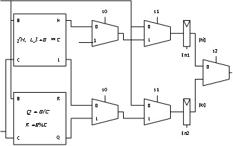
Figure 1: Multiply-divide circuit.
Problem 9. In this assignment you will design an arithmetic logic unit (ALU) which can be used readily in a MIPS processor. In particular, we focus on the arithmetic logic instructions among MIPS R-type instructions. Each machine instruction in a MIPS processor has a 6 bit field called "Funct" (denoted briefly by F here).
A MIPS compatible ALU takes F3:0 as a control input. This control input determines the relation between the data inputs A and B, and the output Y as per Table7, which is a part of the set of MIPS R-type instructions.
A step by step design process is described in the lecture slides. Note that the ALU hardware includes an adder. For this assignment you are free to choose any adder implementation including the behavioural one using System Verilog + operator.
Design an n bit wide parameterized ALU module as per Table7. The ALU should have two additional outputs Cout and
OV to flag the carry out and arithmetic overflow in arithmetic operations.
Create an appropriate top level module to test the ALU circuit on development board.
Marking Criteria: For part (a) the mark is calculated according to the formula fa ∗ ha.
The value of fa depends on the extent to which your circuit is able to meet the specifications. If it satisfies all the requirements, then
fa = 1. If it meets a subset of the specifications then fa < 1, and it will depend on the results achieved.
The value of ha depends on the hardware complexity (i.e. the size of your circuit) of the ALU circuit (excluding the adder/s). See the lecture notes for an economical ALU architecture that will fetch full marks. The maximum value of ha is 4. A behavioral design will get you ha = 3 provided that you can explain the circuit synthesized from your code.
The marks for part (b) will depend on completeness and ease of use of your test scheme.
|
F [3:0]
|
Y
|
|
0000
|
A + B (signed addition)
|
|
0001
|
A + B (unsigned addition)
|
|
0010
|
A - B (signed subtraction)
|
|
0011
|
A - B (unsigned subtraction)
|
|
0100
|
A & B (AND)
|
|
0101
|
A|B (OR)
|
|
0110
|
A ⊕ B (XOR)
|
|
0111
|
(A|B) (NOR)
|
|
1010
|
if(A < B) Y = 1; else Y = 0
|
|
1011
|
if(A < B) Y = 1; else Y = 0 (unsigned comparison)
|
Table 7: Excerpt of MIPS R-type instruction set involving arithmetic-logic operations.