Reference no: EM131460316
Minor corrections:
P1. c: assume for this part that the inverter trip points are at Vbatt/2
P1. f: incorporate the impact of Rin, Cc and Rs in this transfer function
P1. g: your design should absorb the effects of Cc, Rin and Rs.
P3: set VDD=2.5V (not 2V)
P3c: in terms of "N"
P3f: use the same gm, ro as in "c"
P3g: is this a robust design? If not, why not (one sentence)
P4: assume the clock has 2 phases, φ1, φ2
Question 1: The LC buck converter circuit shown takes in a DC voltage Vin, which combines with an AC-coupled triangle wave with peak-to-peak amplitude Vtri, and period T, and then is thresholded by a string of inverters before driving an LC load.
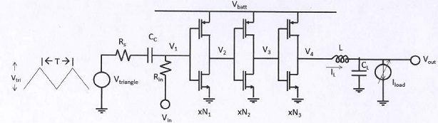
a. Briefly discuss (1 paragraph) the impact/ trade offs of the various components in the circuit. In particular, discuss briefly how the values of L, CL, Cc, Rin, the sizing of the 3 inverters, T, and the ratio Vtri/Vbatt impact: input range, efficiency, and ripple.
The small-signal transfer function (assuming <<√LCL) is:
Vout/Vin = Vbatt/Vtri. (1/(1+ (s/Qωn) + (s/Qωn)2)). (1 + (s/z))/(1 + (s/p))
b. Relate ωn, Q, p and z to L, Cr, Rin, Rtri, Cc, RL (the parasitic resistance of the inductor ) the output conductance of a unit inverter gdsinv and the sizing of the 3 inverters.
ωn= rad/s, Q=
P = rad/s, z= rad/s,
c. Sketch V1-V4, IL and Vout for Vbatt = 3V, Vtri = 2V, Vin = 1V, (assuming << √(LCL) and also assuming IDCout > L.T.Vbatt).
d. Assuming the inverters are sized so that k = μcox W/L is the same for N-and Pfets (so, for the same ID, the have the same Vod), what is the range of Vin that provides linear control of vout, in terms of Vbatt, VTHN and VTHP?
Now, we will want to design a feedback circuit, taking in Vout and a voltage Vref and generating such that when the loop is closed Vout=Vref to within 1%.
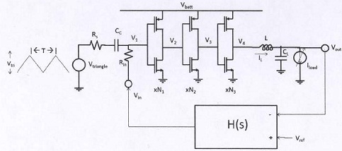
e. Based on the transfer function in (b), what must the feedback DC gain be to achieve 1% accuracy? What, approximately, is the maximum closed-loop bandwidth (essentially UGBW) that can be achieved while still having a reliably stable design? Provide your answers in terms of the coefficients in part (b): ωn, Q, p and z.
H(0)= BW=
f. Design a feedback transfer function, H(s) that provides a closed loop behavior with the desired gain and a bandwidth that approaches the above limit within a factor of 10. Write the coefficients of that transfer function in terms of the coefficients in part (b)
H(s) =
g. Design a circuit to implement the above transfer function. Assume transistors with unit gm = 100μS, unit r0=200kΩ) for Vod = 200mV, Id=10μA, VTH=0.4V. Design for ωn=10Mrad/s, Q=10, Vbatt=3V, Vtri,=2V and Rs=10kΩ. You may choose Cc, and Rin (or incorporate Rin, into the output resistance of your circuit). Critically: the circuit must support an output (Vin) range of 0.5 to 2.5V, and input ("Vout" and Vref) range from 1 to 2V and implement the transfer function from (f) without significantly degrading phase margin of the loop as a whole. Draw the schematic of the circuit, with multiplicities and give the values of any explicit resistors and capacitors, including Cc and Rin.
Question 2:
A 3-stage inveter-style op-amp.
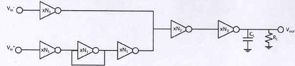
a. For the circuit shown, write the transfer functions Vout/Vin+ and Vout/Vin- in terms of the inverter unit input capacitance, Cinv, transconductance, Ginv, output resistance, Roniv, multiplicities N1, N2, N3, and load RL and CL. Assume the inputs are biased at the trip-point of the inverters (where Vin=Vout). Also, rewrite these transfer functions in terms of differential and common mode inputs.
Vout/Vin- =
Vout/Vin+ =
Vout/Vindiff =
Vout/VinCM =
b. Estimate the differential input referred thermal noise (assume effective y = 1 for an inverter). Which inverters you expect to dominate noise? What is the (approximate) noise in terms of 4kT, unit Gminv, Roinv and N1-N3?
Which components matter?
Vndiff2/HZ=
c. How would you choose N1, N2 and N3 based on input referred noise, RL (for rail-to-rail output), and minimizing current consumption. Describe in words (1 paragraph), supported by equations.
Now, the amplifier is compensated as shown.
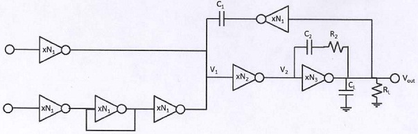
d. Compute the dominant pole and zero at the node between the 2nd and 3rd stages (V2) in terms of C2, N2, N3, CL, RL, Gminv and Roinv.
Assume C2>> N3Cinv, and R2→0. Sketch the Bode plot of the transfer functions V2/V1 and Vout/V1 and lable magnitudes and break frequencies. Hint: this is Miller compensation, so use that style of analysis when figuring out poles and zeros.
p2 =
z2 =
e. Similarly, compute the dominant pole and zero at the node between the 1st and 2nd stages, in terms of N1, C1, Gminv, Roinv and the pole (p2) from, the previous section. Sketch the Bode plot of the transfer functions V1/Vin and Vout/Vin. For simplicity treat the Feedback inverter as an ideal amplifier with gain = GminRoinv, and low output impedance.
f. What purpose does putting R2 in series with C2 serve? Why is there no need for a resistor in series with C1?
g. What benefits does using the feedback inverter provide (list 3 benefits) and why might using it be hard in practice?
Question 3: For the amplifier shown:
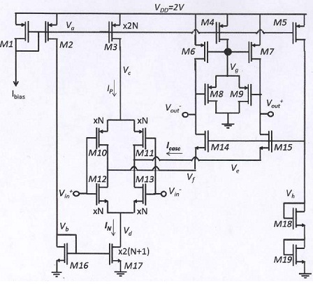
a. What are the DC bias points (node voltages) of the circuit? Assume Vod=0.2V, VTHN=0.4V, VTHP = 0.5V and VDD=2V. Write your answers in terms of Vinal.
Va= , Vb= , Vc= , Vd= , Ve=
Vg= , Vh= , Voutcm=
b. Which transistors act as the following subcomponents:
Differential pair:___
Passive mirror:___
Active mirror:___
Cascode:___
CMFB:___
c. What is the small signal gain of the amplifier shown.? Assume unit gm = 100μS, ro=400kΩ:
ADC=
d. Which components can you ignore when computing noise, and why?
e. What is the input-referred thermal noise, in terms of kT, N and unit gm (assume y=1)
Vin2/Hz = ___
f. What must N be for the input referred noise to be 2nV/Hz1/2?
N = _____
g. For process variation where, VTHN and VTHP vary independently by +/- 100mV (but lbias and Vod are constant) what is the input common mode range that keeps all transistors out of triode across all process corners? For each extreme, state which transistor will enter triode first, and under what process corner.
_____<VinCM<_____
h. If individual component mismatch in VTH is σΔVTH = 8mVμm/(W.L)1/2. What 3-sigma variation in input-referred DC offset can you expect, as a function of N? Assume unit nfets have W/L are 4µm/1µm , and unit pfets have W/L are 16µm/ 1µm
3σVin =
i. Bonus: Applying the same mismatch what 3-sigma variation do you expect in IN? In Ip? What 3-sigma variation do you expect in Icasc.. What is the maximum N allowable that guarantees circuit function under 3-sigma corners of mismatch?
N < _____
Question 4: Open ended design : design, at a transistor level, a circuit that provides a 1.2V (accurate to 50mV) output, able to source up to 50 μA with less than 50mV of droop (so, a 1 kΩ resistance), when powered by a 0.4V supply (typical for a single silicon photovoltaic). Assume transistors with k=μcox = 1mA/V2, gmro = 40.
Assume you have access to a 1MHz clock and a level shifter to set its amplitude to and VDD you can generate. Provide a circuit topology that could reasonably be fully integrated (so, no inductors) and provide critical component values (R's, C's and W/L) as well as critical sizing ratios between transistors, capacitors and/or diodes. Your final schematic must be neat, have different sub-blocks clearly labelled and either clearly indicate component values, or else label each component and have a table listing values.
You may also include 1-2 paragraphs describing your design and reasoning, to increase my chance of understanding/appreciating what you have done. Points will be awarded for functional designs. Bonus points for minimizing current from the 0.4V supply, and for minimum size (based on W,L of large devices, Capacitor values and Resistor values, assuming Lmin=0.25um, wmin of resistors=0.25um, and ρ = 1kΩ/square, and Co = 2fF/μm2). No bonus points if you compute power or area wrong by more than 10%.
IDD = ___μA, Area = ___μm2