Reference no: EM132178377
Digital Electronic System Design - Binary Sequence Detector
Assignment description:
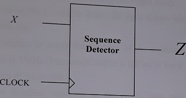
In this assignment, you will design a binary sequence detector using state machine, as shown in the following block diagram, with one input, X, and one output, Z. The detector examines a string of 0's and 1's applied to X, and generates an output Z = 1 only when any input sequence ending in 101110. Z=1 is coincident with the last 0.
The sequence detector has the eight states which are described below. The circuit can be designed by either Moore machine or Mealy machine with the flip-flop type of your choice.
|
Description of states
|
State
|
|
|
Initial state - X doesn't receive an effective bit.
|
SO
|
|
|
X receives one effective bit (1).
|
S1
|
|
|
X receives two effective bits (10).
|
S2
|
|
|
X receives three effective bits (101).
|
S3
|
|
|
X receives four effective bits (1011).
|
S4
|
|
|
X receives five effective bits (10111).
|
S5
|
|
|
S6
|
|
|
X. receives six effective bits (101110).
|
|
Tasks to be carried out:
1. First of all, you should derive a state graph from the above description for your design, which shows transitions of the states of the sequence detector.
2. You should follow the design steps of the sequential logic design to derive the circuit that implement the sequence detector.
3. You are expected to use MAXPLUS II package to capture your design. All files you generate should be placed in your working directory in order that you can use them in the future and nobody else has access to your files.
4. Compile your design and correct any errors that might occur.
5. Edit your waveform file (*.vwf) to define all input signals and to specify the signals you want to view/observe.
6. Simulate your design to verify the function of the sequence detector. Assume that the clock frequency is 1MHz. You should define a full set of input signals to comprehensively test the operation of the circuit.
By the submission deadline indicated on the cover page, you are required to submit a hardcopy of an assignment report (no more than 15 pages), which should include the description of how you design the sequence detector, the schematic captured using MAXPLUS II package, simulation results and discussion/comments on the design, together with your main design files (*.bdf and *.vwf) on a CD/memory stick attached to the report.