Reference no: EM133367297
Question 1. (a) State :
(i) the main disadvantage of an S - R bistable
(ii) the main disadvantage of the D-type bistable.
(b) State an advantage and a disadvantage of the master-slave J - K bistable compared to a basic J - K bistable.
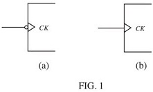
(c) Identify the symbols shown in FIGURES 1 (a) and 1(b).
(d) There are two types of sequential logic circuits that can be classified on the basis of how they are clocked. What are they?
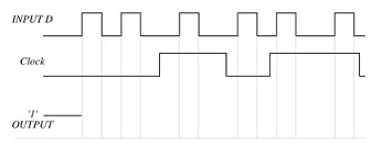
Question 2. (a) The input and clock waveforms for a D-type transparent latch are shown in FIGURE 2. Complete the timing diagram showing the Q output waveform.
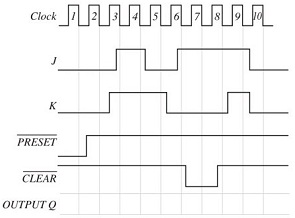
(b) The inputs shown in the timing diagram of FIGURE 3 are applied to a negative edge triggered J - K bistable. Draw the waveform of the output 9 and briefly explain how the states of 9 come about.
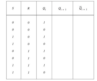
Question 3. FIGURE 4 shows a clocked NAND S - R bistable .
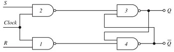
FIG. 4
Complete the truth table shown below and, by constructing a Karnaugh map, show that the next output state after clocking, Qt+1 , is given by the Boolean equation:
Qt+1 = S + Qt,R‾
The states of Qt+1 and Q‾t+1 are not permitted to be the same. Any 'not permitted' states are marked on the Karnaugh map as X, 'don't care'.
Use a Karnaugh map format of:
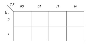
Truth table for a NAND S - R bistable.
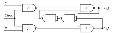
Question 4. lt is found with the circuit of FIGURE 4, that when S = R = 1, and the clock = 1, the outputs are both 1. When the clock reverts to a 0, it is observed that Q always becomes a 1 and Q‾ = 0. If, however, two series NAND gate inverters are inserted in the feedback line from the 9 output to the input of gate 3, as shown in FIGURE 5, then when the clock becomes a 0, Q‾ = 1 and Q = 0.
Briefly explain the reason why this should happen. Assume gates 1 and 4 switch faster than gates 2 and 3.
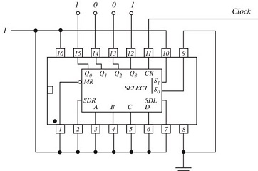
1. FIGURERS 1 , 2 and 3 show respectively the pin connections, logic symbol and IEC symbol ior a sequential device. Identify the device and interpret the IEC symbol.
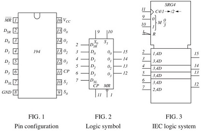
(b) The device of Question 1(a) above is connected as shown in FIGURE 4.
The outputs are Q0 = 1, Q1 = 0, Q2 = 0, Q3 = 1.
Determine the outputs after 2 clock pulses.
2. Design and build a 2-bit Up/Down sequential counter us ing D-type bistables.
The counter must meet the following specification:
• Counter outputs will be 00, 01, 10 and 11
• There is a single input, Y thai controls the direction of the count ihus: V - 0, the counter counts up V = 1, the counter counts down.
• The counter should count up/down from any point in the counting sequence when V changes state.
Your design must show all stages you have used in its development and must be implemented and tested in PSpice and suitable timing waveforms produced.