Reference no: EM132693290
Equipment:
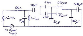
Oscilloscope, function generator, DMM, CD4007 chips, resistances, capacitances. Use measured values of resistances and capacitances. Obtain data sheet for the CD4007 from the internet.
Procedure:
1. The chip CD4007 contains six MOSFET, i.e. 3 n-channel and 3 p-channel MOSFETs connected as shown in Figure-2. The digit by each terminal indicates the pin number on the 14-pin DIP package. Note that pin 14 (E DI)) must always be connected to the most positive power supply voltage, and pin 7 (Vss) must always be connected to the most negative (or ground) power supply voltage in order to keep body-source and body-drain junction from becoming forward biased. This is what provides electrical isolation between the different MOSFETs in the integrated circuit, and if this isolation fails, all of the MOSFETs end up being shorted together with completely unpredictable results. Although it is not shown in the schematic, each of the three inputs to the MOSFET gates (pins 3, 6, & 10) have two electrostatic discharge (ESD) protection diodes that connect them to the VDD and VSS power rails.
For enhancement mode n-MOSFET the gate to source voltage must be positive, and no drain current will flow until Vas exceeds the positive threshold voltage Vt. The MOSFET can be easily damaged by static electricity, be careful in handling the MOSFET.
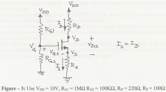
2. Set up circuit for voltage divider biasing shown in Figure-3, and measure ID = Is, VGS, V5, VD, and VDs. Compare with the calculated values of ID, VGS, Vs, VD, and VDS by finding percentage difference between measured and calculated values. What are the sources of difference between the measured and calculated values? Use the n-MOSFET parameters measured in Lab-5, i.e. Vt, ro, gm, VA, K., and remember gm value depends on operating point Q-point. Remember there is no single correct value for Q-point; it will be different depending on the value of Rs, RD and power supply VDD-
3. Using the voltage divider biasing in step-2 set up the circuit for a common gate amplifier shown in Figure-4. Apply an input v,ig 10 mV peak signal at 5 KHz, measure the output peak value vo across load resistance 5Kfl. Find the voltage gain of the amplifier (vo/vmg).
4. Draw small signal equivalent circuit of Figure-4 and calculate the voltage gain expression. Compare the calculated voltage gain Ai, with the measured voltage gain in step-3 by finding the percentage difference.
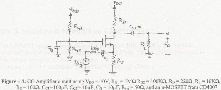
5. Apply an input 10 mV peak signal at 500Hz, measure the output peak value vo across load resistance 51(12. Increase the frequency of the input signal while keeping amplitude the same by step of 1 KHz and find output at each increment of frequency. Present the data in a table showing input signal amplitude, frequency of input signal, output voltage vo amplitude, and gain -- (vo/vsig). Increase the frequency till the output voltage drops below 0.707v0 of the mid-band value, i.e. mid-band is the range of frequencies when output voltage or gain remains the same.