Reference no: EM131523990
Answer the following questions -
Q1. Circuit Analysis
a) Using Mesh analysis:
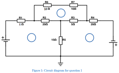
i. Calculate the three mesh currents, I1, I2 and I3, of the network shown in Figure 1,
ii. Calculate the current IR2 through R2,
iii. Calculate the voltage VR5 across R5.
State clearly the directions of the currents and the polarity of the voltage. Show the derivation of the mesh equations. Solve them using a software tool of your choice (e.g. wolframalpha.com) including a screen shot of the results.
The values of V1 and V2 are the last two non-zero digits of your student ID (eg. If your student ID is 7256105, then V1 = 1 and V2=5).

Q2. Operational Amplifiers
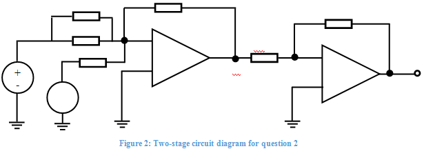
a) The circuit shown in Figure 2 performs the following operation v0 = A1v1 + A2v2 where A1 and A2 are the last two non-zero digits of your student ID:
i) A2 is the smallest digit,
ii) A1 is the largest digit if both digits are different, or, A1 = A2 + 1 if both digits are identical.
(You should always have A1 > A2).
Given that R1 = 1.8 kΩ, Rc = 2 kΩ, Rf2 = 12kΩ, and that R2 = R3, calculate the values for R2 and Rf1 to achieve the desired operation.

Q3. RLC circuits, Resonance and Filters
A RLC series circuit contains a resistance R, an inductor L and a capacitor C. It is driven by a 230 V rms variable frequency AC voltage source. The value of R, C and L are given in Table 1 against the last digit of your student ID.
a) Calculate the resonance frequency (fr) of the circuit and then calculate the following under resonant condition:
i) The individual inductive (XL) and capacitive reactance (XC) and the total impedance (Z) of the circuit.
ii) The circuit current and the voltage across each component.
iii) The power dissipation at the cut-off frequency.
|
Last Digit ofStudent ID
|
R(Ω)
|
L (mH)
|
C(µf)
|
|
0
|
5
|
12
|
4
|
|
1
|
10
|
15
|
2
|
|
2
|
5
|
22
|
6
|
|
3
|
10
|
18
|
8
|
|
4
|
5
|
10
|
10
|
|
5
|
10
|
20
|
7
|
|
6
|
5
|
12
|
24
|
|
7
|
10
|
15
|
10
|
|
8
|
5
|
20
|
8
|
|
9
|
10
|
12
|
14
|
Table 1
Q4. Semiconductor Devices
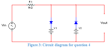
a) In the diode application circuit shown below in Figure 3, the goal is to write an expression for Vout which depends on 3 distinct cases.
a. Case 1: Vin > V1 + VD
b. Case 2: (V2 + VD) < Vin < (V1 + VD)
c. Case 3: Vin < -(V2 + VD)
For a silicon PN junction bias voltage VD = 0.7V, write an expression for Vout for each case.
Set the values of V1 and V2 to be the last two non-zero digits of your student ID.

Q5. Number Systems and Boolean Algebra
a) Assuming that your student ID number is a decimal number, convert it to Hexadecimal and BCD. Please show the workout.
[My student ID is 7546211].