Reference no: EM132206348
Question 1. FIGURE 1 shows a transistor connected in common-emitter mode. Using the Ebers-Moll equations for an npn transistor, estimate the value of the base emitter voltage, VBE, required to make
(i) the collector-emitter voltage, VCE, 5 volts
(ii) the collector current 9.95 mA.
Take ICBS = IEBS = 1 x 10-13 A, αF as 0.98 and keT/e as 25 mV.
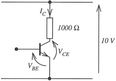
FIG. 1
Question 2. An npn transistor has the doping concentrations as given in TABLE A, where NDE and NDC are the emitter and collector donor concentrations and NAB the acceptor concentration of the base.
FIGURE 2(a) represents the electron and hole carrier densities in the emitter, base and collector for the unbiased transistor.
(a) Justify the assumption made in FIGURE 2(a) that the majority carrier densities nE, nB and nC can be regarded as being the same value as the doping densities NDE, NAB and NDC, respectively.
(b) Determine the values of the unbiased minority carrier densities pE0, nB0 and PC0,
Question 3. FIGURE 2(b) represents the carrier densities in the three neutral regions of the transistor under active conditions. The base-emitter junction is forward-biased by 0.6 volts and the base collector junction is reverse-biased by 1 volt.
The biased minority carrier densities are a function of distance x from the junction interface. In the emitter the minority carrier density is represented by pE(x) and at the emitter-base junction interface by pE(0). Similarly, in the base nB(x) is represented by nB(0) at the emitter-base junction interface. The minority carrier density in the collector is pc(x) and at the base-collector interface is represented by pc(0).
The base-region is sufficiently thin (WB << LN, where LN is the electron diffusion length) as to allow us to assume a linear minority gradient dnB (x)/dx
(a) Calculate the values of pE(0), nB(0) and pc(0).
(b) Estimate the collector current density if the width of the base is 1.1 μm.
(c) Calculate the minimum cross-sectional area of the base if the transistor is to be capable of carrying 1 ampere.
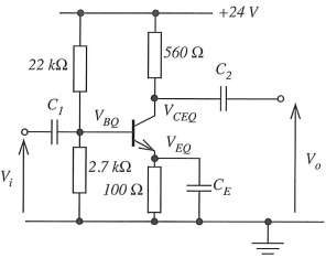
Question 4. Determine the most suitable transistor from TABLE B for use in the circuit of FIGURE 3. You may assume in all cases that the transistor is biased with VBE = 0.6 V.
Attachment:- TMA.rar