Reference no: EM133010496
Objective: Build and simulate a single-stage common-source amplifier using an NMOSFET and a resistor in UMC 130 nm CMOS process.
Steps
1, Build a common source amplifier schematic based on an example in Fig_ 1, Note that VDD is set to 1.2 V The drain resistance, RO, is about 5 1<c) and the load capacitance CO is 1 pF.
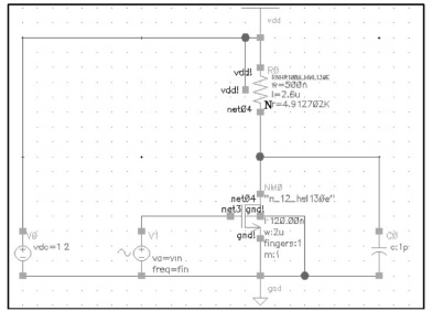
Table I. Components needed
Component Library Category Cell Parameters
|
NMOSFET
|
umcl3mmrf
|
Mos
|
N_12_HSL130E
|
L=120n, w=2u
|
|
Resistor
|
umcl3mmrf
|
Res
|
RNHR1000_MML130E
|
W=500n, I=2.6u
|
|
Capacitor
|
analogLib
|
Passives
|
cap
|
1 pF
|
|
Power supply
|
analogLib
|
SourceslIndependent
|
vdc
|
DC voltage=1.2
|
|
Input signal
|
analogLib
|
Sources[lndependent
|
vsin
|
DC voltage=VG AC magnitude=1 AC phase=0
|
|
VDD pin
|
analogLib
|
SourcesiGlobals
|
vdd
|
|
|
GND pin
|
analogLib
|
SourcesiGlobals
|
gnd
|
|
2. Hand-calculates the DC current and drain voltage using component parameters in table I and process parameters in table II. Assume the gate voltage is 0.6 V.
Table II. Approximate model parameters for hand calculation
Parameter Symbol Value Condition
|
Threshold voltage
|
Vth
|
370m
|
VGS=VDS=0.6 V
|
|
Transconductance parameter
|
KP=pC,,,
|
420u
|
VGS=VDS=0.6 V
|
|
Channel length modulation parameter
|
A
|
0,54
|
VGS=VDS=0.6 V
|
3, Based on DC value obtained from 2 and process parameters in table II
a. Hand-calculate small signal gain.
b, Hand-calculate the pole frequency at the output. (use RO and load capacitance, CO)
4, Set VG to 0.6 V. Perform DC simulation.
a, Find out DC drain current and voltage. (Use Results-Annotate in ADE L)
b, Find out small signal parameters gm and ro (=ligds) (Use Results-Print-DC Operating Points in ADE L)
c. Estimate small-signal gain using the parameters from step b and RO value 5. Set VG to 0.6 V. Perform AC simulation from 1 Hz to 10 GHz.
a, Plot the magnitude (in dB) and phase of drain voltage
b. Find out magnitude and phase at iHz
c. Find out the corner frequency (or pole frequency) where the magnitude is 3 dB lower that that at 1Hz.
d. Find out the unity-gain frequency where the magnitude is 0 dB 6, Compare your hand calculation and simulation results
Report should include
1. Title, name, date
2. Introduction - objectives
3. Schematic captured from the CAD tool for the simulation and its description (take necessary steps to make the schematic capture legible and understandable but do not redraw in Visio or Powerpoint)
4. Required graph plots, and corresponding observations and discussions (make the chart title, axis titles, axis labels clearly legible and understandable)
5. Summary of observations and discussions
6, List of reference (only if cited in the report)
- Follow IEEE two column transactions format attached.
- Do not exceed two pages (excluding references)