Reference no: EM133114961
42092 Advanced Power Electronics - University of Technology Sydney
Lab - Asynchronous and Synchronous Buck and Buck- Boost Converter
Objective 1: To become familiar with asynchronous buck converter.
Objective 2: To become familiar with synchronous buck converter, gate drive requirements and dead- time.
Objective 3: To become familiar with an inverting buck-boost (IBB) converter.
Assessment Part-I:
Asynchronous buck-converter:
Question 1) Using Table 1, calculate the minimum value of inductance L required to keep the asynchronous buck converter (ref. Fig. 1(a)) operation in a Continuous-Conduction Mode (CCM) under all conditions.
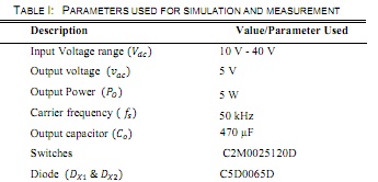
Question 2) Using the calculated value of inductance, model a simple asynchronous buck converter (ref. Fig. 1(a)) in PLECS. Run the simulation (use input voltage of 25V) and plot the gate signal, drain-source voltage of the switch, voltage across the inductor and inductor current in a single scope.
Question 3) Reduce the inductor size to 1/10 of the pre calculated value and run the simulation and plot the gate signal, drain-source voltage of the switch, voltage across the inductor and inductor current in a single scope. What is the difference in waveform compared to Step 2 above. Discuss.
Question 4) In step (2) above, reduce the load to 1/10 of the original and plot the gate signal, drain-source voltage of the switch, voltage across the inductor and inductor current in a single scope. What is the difference in waveform compared to Step 2 above. Discuss.
Question 5) In step (2) above, reduce the switching frequency to 1/10 of the original and plot the gate signal, drain-source voltage of the switch, voltage across the inductor and inductor current in a single scope. What is the difference in waveform compared to Step 2 above. Discuss.
Synchronous buck-converter:
Question 6) Replace the diode with switch to make it synchronous buck-converter converter (ref. Fig. 1(b)). Put complementary signal on the new switch (use a simple NOT gate to generate a complementary pulse). Show the screenshot of the PLECS model.
Question 7) Using Table I and calculated value of L in Step (2), run the simulation and plot the gate signal, drain-source voltage of the switch, voltage across the inductor and inductor current in a single scope.
Question 8) Reduce the inductor size to 1/10 of the pre calculated value and run the simulation and plot the gate signal, drain-source voltage of the switch, voltage across the inductor and inductor current in a single scope. What is the difference in waveform compared to Step 2 above. Discuss.
Question 9) Measure the power loss and efficiency at the rated voltage and power in CCM. Use PLECS.
An inverting buck-boost (IBB) converter:
Question 10) Rewire the circuit as shown in Fig. 3 to make an inverting buck-boost (IBB) converter. Run the simulation (use input voltage of 25 V) and plot the gate signal, drain-source voltage of the switch, voltage across the inductor and inductor current in a single scope.
Question 11) Plot the output voltage vs duty cycle (voltage transfer characteristics) of the switch in Excel. [Hint: measure the output voltage at duty cycle 0.1, 0.2, 0.3, 0.4, 0.5, 0.6, 0.7, 0.8 and plot the output voltage vs duty cycle.]
Simulation file
Question 12) Submit the PLECS simulation file of each:
a) Asynchronous buck dc-dc converter
b) Synchronous buck dc-dc converter.
c) Inverting buck-boost converter.
Attachment:- Advanced Power Electronics.rar