The Zener Diode
We saw that a "reverse biased" diode blocks current in reverse direction, but will suffer from the premature breakdown or damage if reverse voltage applied across it is too high. But, the Zener Diode or "Breakdown Diode" as they are sometimes called, are mainly the same as the standard PN junction diode but are particularly designed to have a low pre-determined Reverse Breakdown Voltage which takes advantage of this high reverse voltage. The point at which the zener diode breaks down or conducts is known as the "Zener Voltage" (Vz).
The Zener diode is like a common-purpose signal diode consisting of the silicon PN junction. When biased in forward direction it behaves like a normal signal diode passing the rated current, but when the reverse voltage is applied to it reverse saturation current remains constant over a broad range of voltages. The reverse voltage increases till the diodes breakdown voltage VB is reached at which point a process called as Avalanche Breakdown takes palce in the depletion layer and current flowing through the zener diode increases dramatically to maximum circuit value (which is commonly limited by a series resistor). This breakdown voltage point is called as "zener voltage" for the zener diodes.
The point at which current flows can be controlled accurately (to less than 1per cent tolerance) in doping stage of the diodes construction giving diode a specific zener breakdown voltage, (Vz) ranging from a few volts up to a few hundred volts. This zener breakdown voltage on the I- V curve is nearly a vertical straight line.
Zener Diode:
Diodes which are designed to work in breakdown region are known as zener diode. If reverse voltage exceeds breakdown voltage, then the zener diode will not be destroyed normally as long as the current does not exceed maximum value and device closes not over load.
When thermally generated carrier (part of the reverse saturation current) falls down the junction and acquires energy of the applied potential, carrier collides with crystal ions and goves sufficient energy to disrupt the covalent bond. Additionally to the original carrier, a new electron-hole pair is generated. This pair can pick up sufficient energy from applied field to collide with the other crystal ion and create still another electron-hole pair. This action carries on and thereby disrupts the covalent bonds. The method is referred to as impact ionization, avalanche multiplication or the avalanche breakdown.
There is a second mechanism which disrupts covalent bonds. The use of the sufficiently strong electric field at junction can create a direct rupture of bond. If electric field exerts a strong force on a bound electron, electron can be torn from covalent bond hence causing the number of electron-hole pair combinations to multiply. This mechanism is called as high field emission or Zener breakdown. The value of reverse voltage at which this takes place is controlled by amount of doping of the diode. A heavily doped diode has a low Zener breakdown voltage, while the lightly doped diode has a high Zener breakdown voltage.
At voltages above nearly 8V, the predominant mechanism is the avalanche breakdown. Since the Zener effect (avalanche) take place at a predictable point, the diode can be used as a voltage reference. The reverse voltage at which the avalanche takes place is called as breakdown or Zener voltage.
A Zener diode characteristic is shown in figure. The circuit symbol for Zener diode is different from that of regular diode, and is illustrated in figure. Maximum reverse current, IZ(max), which Zener diode can withstand is dependent on design and construction of the diode. A design guideline that the minimum Zener current, where the characteristic curve remains at VZ is 0.1/ IZ(max).
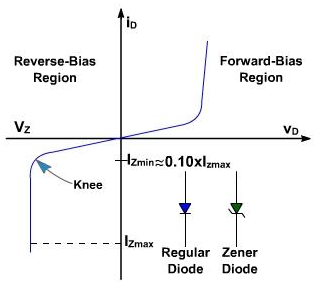
Figure 1 - Zener diode characteristic
Power handling capacity of these diodes is much better. The power dissipation of zener diode equals to the product of its voltage and current.
PZ= VZ IZ
The amount of the power which zener diode can withstand ( VZ.IZ(max) ) is a limiting factor in the power supply design.
Email based Electronics Devices and circuits assignment help - homework help at Expertsmind
Are you searching Electronics Engineering assignment help expert for help with Zener Diodes questions? Zener Diodes topic is not easier to learn without any external help? We at www.expertsmind.com offers free lecture notes for Electronics Devices and circuits assignment help and Electronics Devices and circuits homework help. Live tutors are available 24x7 hours for helping students in their Zener Diodes related problems. We provide step by step Zener Diodes question's answers with 100% plagiarism free content. We prepare quality content and notes for Zener Diodes topic under Electronics Devices and circuits theory and study material. These are avail for subscribed users and they can get advantages anytime.
Why Expertsmind for assignment help
- Higher degree holder and experienced experts network
- Punctuality and responsibility of work
- Quality solution with 100% plagiarism free answers
- Time on Delivery
- Privacy of information and details
- Excellence in solving electronics engineering questions in excels and word format.
- Best tutoring assistance 24x7 hours