Biasing the Field Effect Transistor
Voltage Divider Bias :
The biasing circuit is based on the single power supply is shown in the figure 1. This is like the voltage divider bias used with the bipolar transistor.
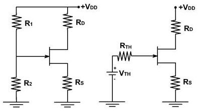
Figure 1
The Thevenin voltage VTH which is applied to the gate is
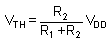
The Thevenin resistance can be given as

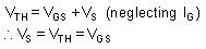
The gate current is supposed to be negligible. VTH is the DC voltage from gate to ground.
The drain current ID can be given by

and the dc voltage from the drain to ground is VD = VDD - ID RD.
If the value of VTH is large enough to swamp out VGS the drain current is approximately constant for any JFET as shown in the figure 2.
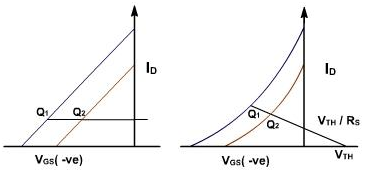
Figure 2
There is a problem in JFET. In a BJT, VBE is approximately 0.7V, with only minor variations from one transistor to other. In the FET, VGS can vary some volts from one JFET to another. It is thus, difficult to make VTH large enough to swamp out VGS. For this very reason, the voltage divider bias is less effective with, FET than the BJT. Hence, VGS is not negligible. The current increases slightly from Q2 to Q1. However, voltage divider bias maintains ID nearly constant.
Consider the voltage divider bias circuit as shown in the figure 3.
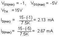
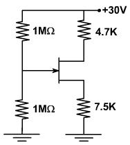
Difference in ID (min) and ID (max) is less
VD (max) = 30 - 2.13 * 4.7 = 20 V VD (min) = 30 - 2.67 * 4.7 = 17.5 V
Email based Electronics Devices and circuits assignment help - homework help at Expertsmind
Are you searching Electronics Engineering assignment help expert for help with Voltage Divider Bias questions? Voltage Divider Bias topic is not easier to learn without any external help? We at www.expertsmind.com offers free lecture notes for Electronics Devices and circuits assignment help and Electronics Devices and circuits homework help. Live tutors are available 24x7 hours for helping students in their Voltage Divider Bias related problems. We provide step by step Voltage Divider Bias question's answers with 100% plagiarism free content. We prepare quality content and notes for Voltage Divider Bias topic under Electronics Devices and circuits theory and study material. These are avail for subscribed users and they can get advantages anytime.
Why Expertsmind for assignment help
- Higher degree holder and experienced experts network
- Punctuality and responsibility of work
- Quality solution with 100% plagiarism free answers
- Time on Delivery
- Privacy of information and details
- Excellence in solving electronics engineering questions in excels and word format.
- Best tutoring assistance 24x7 hours