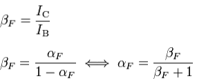
Transistor 'alpha' and 'beta'
The proportion of the electrons able to cross the base and reach the collector is a measure of BJT efficiency. The heavy doping of emitter region and light doping of base region cause a number of electrons to be injected from emitter into the base than holes to be injected from the base into emitter. The common-emitter current gain can be represented by βF or hfe; it is approximately the ratio of DC collector current to DC base current in the forward-active region. It is typically larger than 100 for small-signal transistors but can be very small in transistors designed for high power applications. Another significant parameter is the common-base current gain, αF. The common-base current gain is the gain of current from the emitter to collector in forward-active region. This ratio has a value close to unity; in between 0.98 and 0.998. Alpha and beta are precisely related by the following identities

Structure
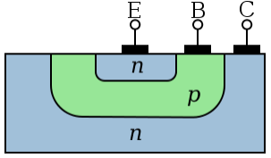
The simplified cross section of the planar NPN bipolar junction transistor
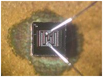
High-frequency NPN transistor, base and emitter connected via bonded wires
A BJT consists of 3 differently doped semiconductor regions, the base region, the emitter region, and collector region. These regions are, respectively, n type, p type, and p type in a PNP, and p type, n type, and n type in a NPN transistor. Each semiconductor region is connected to the terminal, appropriately labeled: base (B), emitter (E), and collector (C).
The base is physically located in between the emitter and the collector and is made from slightly doped, high resistivity material. The collector surrounds emitter region, making it almost impossible for electrons injected into base region to escape being collected, therefore making the resulting value of α very close to unity, and so, giving the transistor a large β. A cross section view of the BJT indicates that the collector-base junction has a quite larger area than the emitter- base junction.
The bipolar junction transistor, not like other transistors, is not a symmetrical device. This means that interchanging the collector and emitter makes transistor leave the forward active mode and begin to operate in the reverse mode. Because the transistor's internal structure is generally optimized for the forward-mode operation, interchanging collector and the emitter makes values of α and β in the reverse operation smaller than those in the forward operation; the α of the reverse mode is less than 0.5. The lack of symmetry is primarily because of the doping ratios of the emitter and collector. The emitter is doped heavily, while t he collector is lightly doped, allowing the large reverse bias voltage to be applied before collector-base junction breaks down. The collector-base junction is reverse biased in the normal operation. The reason the emitter is heavily doped is to increase emitter injection efficiency: ratio of the carriers injected by emitter to those injected by base. For the high current gain, most of the carriers injected into emitter-base junction must come from emitter.
The low-performance "lateral" bipolar transistors used in CMOS processes are sometimes designed symmetrically, i.e., with no difference in between forward and backward operation.
Small changes in voltage applied across base-emitter terminals causes the current which flows between the emitter and collector to change considerably. The effect can be used to amplify input voltage or current. The BJTs can be thought of as voltage controlled current sources, but are simply characterized as current controlled current amplifiers, or current sources, because of the low impedance at base.
Early transistors were made from the germanium but most modern BJTs are made from The significant minority are also now made from gallium arsenide, especially for high speed applications
Email based Electronics Devices and circuits assignment help - homework help at Expertsmind
Are you searching Electronics Engineering assignment help expert for help with Transistor 'alpha' and 'beta' questions? Transistor 'alpha' and 'beta' topic is not easier to learn without any external help? We at www.expertsmind.com offers free lecture notes for Electronics Devices and circuits assignment help and Electronics Devices and circuits homework help. Live tutors are available 24x7 hours for helping students in their Transistor 'alpha' and 'beta' related problems. We provide step by step Transistor 'alpha' and 'beta' question's answers with 100% plagiarism free content. We prepare quality content and notes for Transistor 'alpha' and 'beta' topic under Electronics Devices and circuits theory and study material. These are avail for subscribed users and they can get advantages anytime.
Why Expertsmind for assignment help
- Higher degree holder and experienced experts network
- Punctuality and responsibility of work
- Quality solution with 100% plagiarism free answers
- Time on Delivery
- Privacy of information and details
- Excellence in solving electronics engineering questions in excels and word format.
- Best tutoring assistance 24x7 hours