Space charge capacitance CT of diode:
Reverse bias makes the majority carriers to move away from junction, thereby creating more ions. Thus the thickness of depletion region increases. The region acts as a dielectric material used for making capacitors. The P type and N type conducting on each side of dielectric behaves as the plate. The incremental capacitance CT can be defined as

Since 
Thus,  (E-1)
(E-1)
here, dQ is increase in charge caused by change dV in voltage. CT is not constant, it depends on the applied voltage, thus it can be defined as dQ / dV.
When PN junction is forward biased, then the capacitance defined called as diffusion capacitance CD (the rate of change of injected charge with the voltage) to take in account the time delay in moving the charges across junction by diffusion method. It is basically considered as the fictitious element which lets us to predict time delay.
If amount of charge to be moved across the junction is increased, the time delay is greater, it follows that diffusion capacitance varies directly with the magnitude of forward current.
 (E-2)
(E-2)
Relationship between Diode Current and Diode Voltage
The exponential relationship exists among carrier density and applied potential of diode junction as given in the equation E-3. This exponential relationship of the current iD and voltage vD holds over the range of at least 7 orders of magnitudes of current that is a factor of 107.
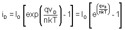 (E-3)
(E-3)
Where,
iD= Current through the diode
vD= Potential difference across the diode terminals
IO= Reverse saturation current
q = Electron charge: 1.60 x 10⁻¹⁹ joules/volt k = Boltzmann's constant: 1.38 x l0-23 joules /° T = Absolute temperature in degrees Kelvin
n = Empirical scaling constant between 0.5 and 2, referred to as the Exponential sometimes
Ideality Factor
The empirical constant, n, is a number that can vary according to the voltage and current levels. It is dependent on electron diffusion, drift, and carrier recombination in depletion region. The quantities which are affecting the value of n are the diode manufacture, levels of doping and purity of materials. If n=1, value of k T/ q is 26 mV at the temperature 25°C. When n=2, k T/ q becomes 52 mV.
For the germanium diodes, n is generally considered to be close to 1. For the silicon diodes, n is in
range of 1.3 to 1.6. n is assumed 1 for all junctions all throughout unless otherwise noted. Equation (E-3) can be simplified by defining VT =k T/q, yielding
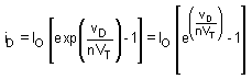 (E-4)
(E-4)
At room temperature (25°C) with forward-bias voltage only the first term in the parentheses is dominant and the current is approximately given by
 (E-5)
(E-5)
The current-voltage (l-V) characteristic of diode, as defined by (E-3) is shown in the figure 1. The curve in the figure given consists of two exponential curves. The exponent values are so that for the voltages and currents experienced in practical circuits, curve sections are close to being straight lines. For the voltages less than VON, curve is approximated by a straight line of slope near to zero. As the slope is the conductance (that is i / v), the conductance is quite small in this region, and equivalent resistance is quite high. For voltages above VON, the curve is approximated by straight line with the quite large slope. The conductance is thus very large, and the diode has small equivalent resistance.
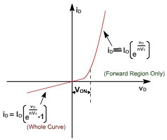
Fig.1 - Diode Voltage relationship
The slope of the curves of fig.1 changes as the current and voltage change since the l-V characteristic follows the exponential relationship of relationship of equation (E-4). Differentiate the equation (E-4) to find the slope at any arbitrary value of vD or iD,
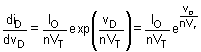 (E-6)
(E-6)
The slope given is the equivalent to the conductance of diode at the specified values of vD or iD.
We can approximate the slope as a linear function of the diode current. To remove the exponential function, we substitute equation (E-4) into the exponential of equation (E-7) to obtain
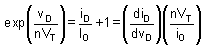 (E-7)
(E-7)
The assumption is that IO<< iD equation (E-7) then yields,
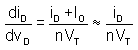 (E-8)
(E-8)
The approximation applies if the diode is forward biased. The dynamic resistance is reciprocal of this expression.
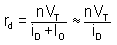 (E-9)
(E-9)
Although rd is a function of id, we can approximate it as a constant if the variation of iD is small. It corresponds to approximating the exponential function as a straight line within the specific operating range.
Generally, the term Rf to denote diode forward resistance. Rf is composed of the rd and contact resistance. Contact resistance is a relatively small resistance composed of resistance of the actual connection to diode and the resistance of semiconductor prior to junction. The reverse-bias resistance is extremely large and is usually approximated as infinity.
Email based Electronics Devices and circuits assignment help - homework help at Expertsmind
Are you searching Electronics Engineering assignment help expert for help with Space charge capacitance CT of diode questions? Space charge capacitance CT of diode topic is not easier to learn without any external help? We at www.expertsmind.com offers free lecture notes for Electronics Devices and circuits assignment help and Electronics Devices and circuits homework help. Live tutors are available 24x7 hours for helping students in their Space charge capacitance CT of diode related problems. We provide step by step Space charge capacitance CT of diode question's answers with 100% plagiarism free content. We prepare quality content and notes for Space charge capacitance CT of diode topic under Electronics Devices and circuits theory and study material. These are avail for subscribed users and they can get advantages anytime.
Why Expertsmind for assignment help
- Higher degree holder and experienced experts network
- Punctuality and responsibility of work
- Quality solution with 100% plagiarism free answers
- Time on Delivery
- Privacy of information and details
- Excellence in solving electronics engineering questions in excels and word format.
- Best tutoring assistance 24x7 hours