Small Signal CE Amplifiers:
CE amplifiers are quite popular to amplify the small signal AC. After the transistor has been biased with the Q point near the middle of a DC load line, AC source can be coupled to the base. This produces fluctuations in base current and hence in collector current of same shape and frequency. Output will be enlarged in sine wave of same frequency.
The amplifier is called linear if it does not change the wave shape of the signal. As long as the input signal is small, the transistor will use a small part of the load line only and the operation will be linear in nature.
On the other hand, if input signal is too large. The fluctuations along load line will drive the transistor into saturation or cut off. This clips the peaks of input and amplifier is no longer linear in nature.
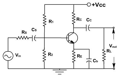
The CE amplifier configuration is shown in the figure 1.

Figure 1
The coupling capacitor (CC ) passes an AC signal from one point to another point. At the same time it does not permit the DC to pass through it. Hence it is called blocking capacitor also.

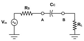
Figure 2
For instance in figure 2, the AC voltage at point A is transmitted to point B. For this series reactance XC should be quite small as compared to series resistance RS. The circuit to the left of A can be a source and a series resistor or can be the Thevenin equivalent of the complex circuit. Similarly RL can be the load resistance or equivalent resistance of the complex network. The current in loop can be given by

As the frequency increases,  decreases, and current increases until it reaches to its maximum value vin / R. Therefore capacitor couples the signal properly from A to B when XC<< R. The size of coupling capacitor depends upon lowest frequency to be coupled. Normally, for the lowest frequency XC ≤0.1R is taken as design rule.
The coupling capacitor behaves like a switch, which is open to DC and shorted for AC.
The bypass capacitor Cb is similar to coupling capacitor, except that it couples an ungrounded point to the grounded point. The Cb capacitor looks like a short to an AC signal and hence emitter is said AC grounded. A bypass capacitor does not disturb the DC voltage at emitter because it looks open to DC current. As a design rule XCb ≤ 0.1RE at the lowest frequency.
Email based Electronics Devices and circuits assignment help - homework help at Expertsmind
Are you searching Electronics Engineering assignment help expert for help with Small Signal CE Amplifiers questions? Small Signal CE Amplifiers topic is not easier to learn without any external help? We at www.expertsmind.com offers free lecture notes for Electronics Devices and circuits assignment help and Electronics Devices and circuits homework help. Live tutors are available 24x7 hours for helping students in their Small Signal CE Amplifiers related problems. We provide step by step Small Signal CE Amplifiers question's answers with 100% plagiarism free content. We prepare quality content and notes for Small Signal CE Amplifiers topic under Electronics Devices and circuits theory and study material. These are avail for subscribed users and they can get advantages anytime.
Why Expertsmind for assignment help
- Higher degree holder and experienced experts network
- Punctuality and responsibility of work
- Quality solution with 100% plagiarism free answers
- Time on Delivery
- Privacy of information and details
- Excellence in solving electronics engineering questions in excels and word format.
- Best tutoring assistance 24x7 hours