Biasing the Field Effect Transistor
Self Bias:
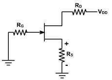
Figure 1, shows a self bias circuit another manner by which we can bias a FET. The drain supply is used only and no gate supply. The basic idea is to make use the voltage across RS to produce the gate source reverse voltage.
This is the form of a local feedback which is similar to that which we use with bipolar transistors. If we increases drain current, the voltage drop across RS increases as the ID RS increases. This increases gate source reverse voltage which makes the channel narrow and reduces drain current. The overall effect is to offset the original increase in drain current. Likewise, if ID Figure 1 decreases, drop across RS decreases, hence the reverse bias decreases and ID increases.
As the gate source junction is made reverse biased, negligible the gate current flows through RG and so the gate voltage with respect to the ground is zero.
VG= 0;
The source to ground voltage equals the product of drain current and source resistance.
\ VS= ID R S.
The gate source voltage is difference in between the gate voltage and the source voltage. VGS = VG - VS = 0 - IDRS
VGS = -ID RS.
This means that the gate source voltage equals the negative of the voltage across the source resistor. The greater the value of drain current, more negative the gate source voltage becomes.
By rearranging the equation: ID = -VGS / RS
The graph of this equation is called as self base line a shown in the figure 2.
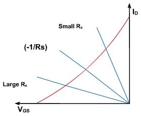
Figure 2
The operating point on the transductance curve is intersection of the self bias line and transductance curve. The slope of line is (-1 / RS). If the source resistance is large (-1 / RS is small) then Q-point is far down the transductance curve and drain current is small. When the value of RS is small, the Q point is far up the transductance curve and drain current is large. In between there exist an optimum value of RS which sets up a Q point near the middle of the transductance curve.
The transductance curve ranges widely for FET (due to the variation in IDSS and VGS(off)) as shown in the figure 3. The actual curve can be between there extremes. A and B are optimum points for the 2 extreme curves. To find out the optimum resistance RS, so that the Q-point is accurate for all the curves, A and B points are joined so that it passes through the origin.
The slope of this line provides the resistance value RS( VGS = -ID RS). The current IQ is such that IA > IQ > IB. Here A, Q and B all points are in the straight line.
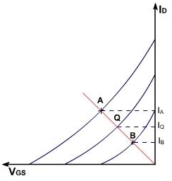
Fig. 3
By taking the case where a line drawn to pass in between points A and B does not pass through the origin. The equation VGS = - ID RS is not appropriate. The equation of the line is VGS = VGG - ID RS.
This type of a bias relationship can be obtained by adding a fixed bias to the gate in addition to the source self bias as shown in the figure 4.
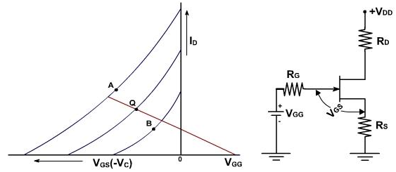
Figure 4
In the circuit
VGG = RS IG + VGS + ID RS
Since RS IG = 0;
VGG = VGS + ID RS
or VGS = VGG- ID RS
Email based Electronics Devices and circuits assignment help - homework help at Expertsmind
Are you searching Electronics Engineering assignment help expert for help with Self Bias questions? Self Bias topic is not easier to learn without any external help? We at www.expertsmind.com offers free lecture notes for Electronics Devices and circuits assignment help and Electronics Devices and circuits homework help. Live tutors are available 24x7 hours for helping students in their Self Bias related problems. We provide step by step Self Bias question's answers with 100% plagiarism free content. We prepare quality content and notes for Self Bias topic under Electronics Devices and circuits theory and study material. These are avail for subscribed users and they can get advantages anytime.
Why Expertsmind for assignment help
- Higher degree holder and experienced experts network
- Punctuality and responsibility of work
- Quality solution with 100% plagiarism free answers
- Time on Delivery
- Privacy of information and details
- Excellence in solving electronics engineering questions in excels and word format.
- Best tutoring assistance 24x7 hours