Reverse Bias:
If the positive terminal of DC source is connected to cathode and negative terminal is connected to anode, the diode biased as shown in figure1.
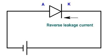
Figure1
When diode is reverse biased then the depletion region width increases, majority carriers move away from there is no flow of current because of majority carriers but there are thermally produced electron hole pair also. If the holes are generated in the locality of junction then there is the flow of current. The negative voltage applied to attract the holes hence generated and repel electrons. At the same time, the positive voltage will attract the electrons battery and repel the holes. This will make current to flow in the circuit. This current is usually quite small. Since this current is because of minority carriers and these number of minority carriers are fixed at a therefore, the current is almost constant known as reverse saturation current ICO.
In an actual diode, the current is not almost constant but increases slightly with the voltage. This is due to surface lea surface of the diode follows ohmic law V=IR. The resistance under reverse bias condition is very high 100k to m the reverse voltage is increased, then at certain voltage, then breakdown to diode takes place and it conducts he to avalanche or zener breakdown. The characteristic of diode is shown in the figure2.
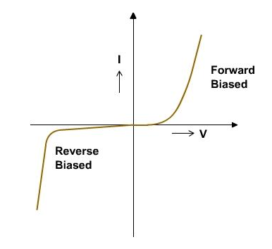
Fig.2
Forward bias:
When the diode is forward bias, then majority carriers are pushed towards the junction, when they collide and replace each other. Numbers of majority carriers are fixed in the semiconductor. Thus as each electron is eliminated at electron should be introduced, this comes from the battery. At same time, one hole should be created in P layer. Extracting one of the electron from P layer. Hence, there is a flow of carriers and thus the flow of current.
Email based Electronics Devices and circuits assignment help - homework help at Expertsmind
Are you searching Electronics Engineering assignment help expert for help with Reverse Bias and forward bias P-N Junction Diode questions? Reverse Bias and forward bias P-N Junction Diode topic is not easier to learn without any external help? We at www.expertsmind.com offers free lecture notes for Electronics Devices and circuits assignment help and Electronics Devices and circuits homework help. Live tutors are available 24x7 hours for helping students in their Reverse Bias and forward bias P-N Junction Diode related problems. We provide step by step Reverse Bias and forward bias P-N Junction Diode question's answers with 100% plagiarism free content. We prepare quality content and notes for Reverse Bias and forward bias P-N Junction Diode topic under Electronics Devices and circuits theory and study material. These are avail for subscribed users and they can get advantages anytime.
Why Expertsmind for assignment help
- Higher degree holder and experienced experts network
- Punctuality and responsibility of work
- Quality solution with 100% plagiarism free answers
- Time on Delivery
- Privacy of information and details
- Excellence in solving electronics engineering questions in excels and word format.
- Best tutoring assistance 24x7 hours