PN junction Distance
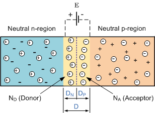
As N-type material has lost electrons and P-type has lost holes, the N-type substance has become positive with respect to P-type. Then the presence of impurity ions on both the sides of junction causes electric field to be established across this region with N-side at the positive voltage relative to P-side. The problem which occurs now is that a free charge requires some extra energy to overcome the barrier which now exists for it to be able to cross the depletion region junction.
This electric field created by diffusion process has generated a "built-in potential difference" across junction with an open-circuit (zero bias) potential of:
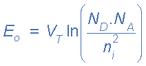
Here: Eo is zero bias junction voltage, VT thermal voltage of 26mV at room temperature, ND and NA are the impurity concentrations and ni is the intrinsic concentration.
A suitable positive voltage (forward bias) applied between two ends of the PN junction can supply the free electrons and holes with extra energy. The external voltage needed to overcome this potential barrier which now exists is very much dependent upon type of the semiconductor material used and the actual temperature of it. Typically at room temperature the voltage across the depletion layer for silicon is around 0.6 - 0.7 volts and for germanium is around 0.3 - 0.35 volts. This potential barrier will always exist even if the device is not connected to any external power source.
The importance of this built in potential across junction, is that it opposes flow of the holes and electrons across the junction and is why it is known as the potential barrier. In practice, a PN junction is formed within the single crystal of material rather than just joining or fusing together 2 separate pieces. Electrical contacts are also fused onto each side of crystal to allow an electrical connection to be made to the external circuit. Resulting device which has been made is known as PN junction Diode or Signal Diode.
In next topic about the PN junction, we will look at the most interesting aspects of PN junction is its use in circuits as a diode. By adding connections to each end of P-type and N-type materials we can produce a 2 terminal device known as PN Junction Diode which can be biased by external voltage to either block or allow the flow of the current through it.
Email based Electronics Devices and circuits assignment help - homework help at Expertsmind
Are you searching Electronics Engineering assignment help expert for help with PN Junction Distance questions? PN Junction Distance topic is not easier to learn without any external help? We at www.expertsmind.com offers free lecture notes for Electronics Devices and circuits assignment help and Electronics Devices and circuits homework help. Live tutors are available 24x7 hours for helping students in their PN Junction Distance related problems. We provide step by step PN Junction Distance question's answers with 100% plagiarism free content. We prepare quality content and notes for PN Junction Distance topic under Electronics Devices and circuits theory and study material. These are avail for subscribed users and they can get advantages anytime.
Why Expertsmind for assignment help
- Higher degree holder and experienced experts network
- Punctuality and responsibility of work
- Quality solution with 100% plagiarism free answers
- Time on Delivery
- Privacy of information and details
- Excellence in solving electronics engineering questions in excels and word format.
- Best tutoring assistance 24x7 hours