The PN junction
In the earlier tutorial we saw how to make the N-type semiconductor material by doping it with the Antimony and also how to make a P-type semiconductor material by doping with the Boron. This is good, but these semiconductor N and P-type materials do very small on their own as they are neutral electrically, but when we join them together these two materials behave in a quite different way producing what is commonly known as a PN Junction.
When N and P-type semiconductor materials are joined together first a very large density gradient is there in between both sides of the junction so some free electrons from the donor impurity atoms start to migrate across this newly formed junction to fill up the holes in P- type material producing the negative ions. Although, because the electrons have moved across the junction from N-type silicon to P-type silicon, they leave behind the positively charged donor ions (ND) on negative side and now holes from the acceptor impurity migrate across the junction in the opposite direction into region where there are large free electrons. As a result of which, the charge density of the P-type along with the junction is filled with the negatively charged acceptor ions (NA), and charge density of the N-type along with the junction becomes positive. This charge transfer of the electrons and holes across the junction is called as diffusion.
This process continues back and forth until the number of electrons which have crossed the junction have a large enough electrical charge to repel or prevent any more carriers from crossing the junction. The regions on both sides of the junction become depleted of any free carriers in comparison to the N and P type materials away from the junction. Eventually a state of equilibrium (electrically neutral situation) will occur producing a "potential barrier" zone around the area of the junction as the donor atoms repel the holes and the acceptor atoms repel the electrons. Since no free charge carriers can rest in a position where there is a potential barrier the regions on both sides of the junction become depleted of any more free carriers in comparison to the N and P type materials away from the junction. This area around the junction is now called the Depletion Layer.
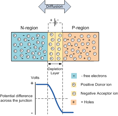
The total charge on each side of junction should be equal and opposite to maintain the neutral charge condition around the junction. If depletion layer region has the distance D, it then must penetrate into the silicon by the distance Dp for the positive side, and a distance Dn for the negative side giving a relationship between two of Dp.NA = Dn.ND in order to maintain the charge neutrality also called as equilibrium.
Email based Digital Electronics assignment help - homework help at Expertsmind
Are you searching Electronics Engineering assignment help expert for help with PN junction questions? PN junction topic is not easier to learn without any external help? We at www.expertsmind.com offers free lecture notes for Digital Electronics assignment help and Digital Electronics homework help. Live tutors are available 24x7 hours for helping students in their PN junction related problems. We provide step by step PN junction question's answers with 100% plagiarism free content. We prepare quality content and notes for PN junction topic under digital electronics theory and study material. These are avail for subscribed users and they can get advantages anytime.
Why Expertsmind for assignment help
- Higher degree holder and experienced experts network
- Punctuality and responsibility of work
- Quality solution with 100% plagiarism free answers
- Time on Delivery
- Privacy of information and details
- Excellence in solving electronics engineering questions in excels and word format.
- Best tutoring assistance 24x7 hours