P-N Junction Diode:
The pure silicon crystal or germanium crystal is generally called as an intrinsic semiconductor. There are not sufficient free electrons and holes in an intrinsic semi-conductor to obtain a usable current. Electrical action of these can be modified by doping means adding impurity atoms to a crystal to increase the number of free holes or no of free electrons.
When the crystal has been doped, it is called as extrinsic semi-conductor. They are generally of two types
• N type semiconductor with free electrons as majority carriers
• P type semiconductor with free holes as majority carriers
These doped materials are of little use, by themselves. However, if the junction is made by joining P type semiconductor to N type semiconductor a useful device is produced called as diode. It will let the current to flow through it only in one direction. The unidirectional properties of the diode allow the current to flow when forward biased and disallow the current to flow when reversed biased. This process is called as rectification and thus it is also called rectifier.
How can it be possible that by properly joining the two semiconductors each of which, by itself, will freely conduct current in any direct refuses to allow the conduction in one direction.
Consider first the condition of P type and N type germanium just prior to joining figure. The majority and minority carriers are in the constant motion.
The minority carriers are thermally produced and they exist only for the short time duration after which they recombine and neutralize each other. In mean time, the other minority carriers have been produced and this process continues.
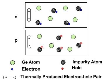
The number of these electron hole pair which exist at any one time depends upon temperature. The Fig number of majority carriers is, fixed depending upon the number of impurity atoms available. While electrons and holes are in the motion but the atoms are fixed in place and do not move at all.
As soon as, the junction is formed, the processes are initiated.
• Holes from the P side diffuse into N side where they recombine with the free electrons.
• The free electrons from N side diffuse into P side where they recombine with the free holes.
• The diffusion of electrons and holes is because of the fact that large number of electrons are concentrated in one area and large number of holes are concentrated in another area.
• When these electrons and holes starts diffusing across the junction then they collide each other and the negative charge in electrons cancels the positive charge of hole and both will lose their charges.
• Diffusion of the holes and electrons is an electric current known as recombination current. The recombination process decompose exponentially with time and distance both from the junction. Therefore most of the recombination takes place just after the junction is made and near to the junction.
• A measure of rate of the recombination is lifetime defined as time needed for the density of carriers to decrease to 37 per cent to the original concentration
The impurity atoms are fixed at their specific places. The atoms itself are the part of crystal and so cannot move. When electrons and hole meet, their individual charge is cancelled and this leaves originating impurity atoms with the net charge, the atom which produced the electron now lack an electronic and so becomes positively charged, whereas the atoms which produced the hole now lacks the positive charge and becomes negative.
Electrically charged atoms are called as ions as they are no longer neutral. These ions produce an electric field. After the several collisions take place, the electric field is large enough to the repel rest of majority carriers away from the junction. For instance, the electron trying to diffuse from N to P side is repelled by negative charge of the P side. Thus process of diffusion does not continue indefinitely but continues as long as the field is developed.
This region is produced immediately surrounding the junction that has no majority carriers. The majority carriers have been repelled away from the junction and junction is depleted from carriers. The junction is called as the barrier region or depletion region. The electric field represents the potential difference across junction also called as space charge potential or barrier potential. This potential is 0.7v for Si at 25o celcious and 0.3v for Ge.
The physical width of depletion region depends on doping level. If heavy doping is used, the depletion region is physically thin as diffusion charge need not travel far across the junction before the recombination occur (short life time). If doping is light, then depletion is wider (long life time).
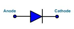
The symbol of diode is shown in the figure 2. The terminal connected to P layer is called anode (A) and the terminal N layer is called as cathode (K)
Email based Electronics Devices and circuits assignment help - homework help at Expertsmind
Are you searching Electronics Engineering assignment help expert for help with P-N Junction Diode questions? P-N Junction Diode topic is not easier to learn without any external help? We at www.expertsmind.com offers free lecture notes for Electronics Devices and circuits assignment help and Electronics Devices and circuits homework help. Live tutors are available 24x7 hours for helping students in their P-N Junction Diode related problems. We provide step by step P-N Junction Diode question's answers with 100% plagiarism free content. We prepare quality content and notes for P-N Junction Diode topic under Electronics Devices and circuits theory and study material. These are avail for subscribed users and they can get advantages anytime.
Why Expertsmind for assignment help
- Higher degree holder and experienced experts network
- Punctuality and responsibility of work
- Quality solution with 100% plagiarism free answers
- Time on Delivery
- Privacy of information and details
- Excellence in solving electronics engineering questions in excels and word format.
- Best tutoring assistance 24x7 hours